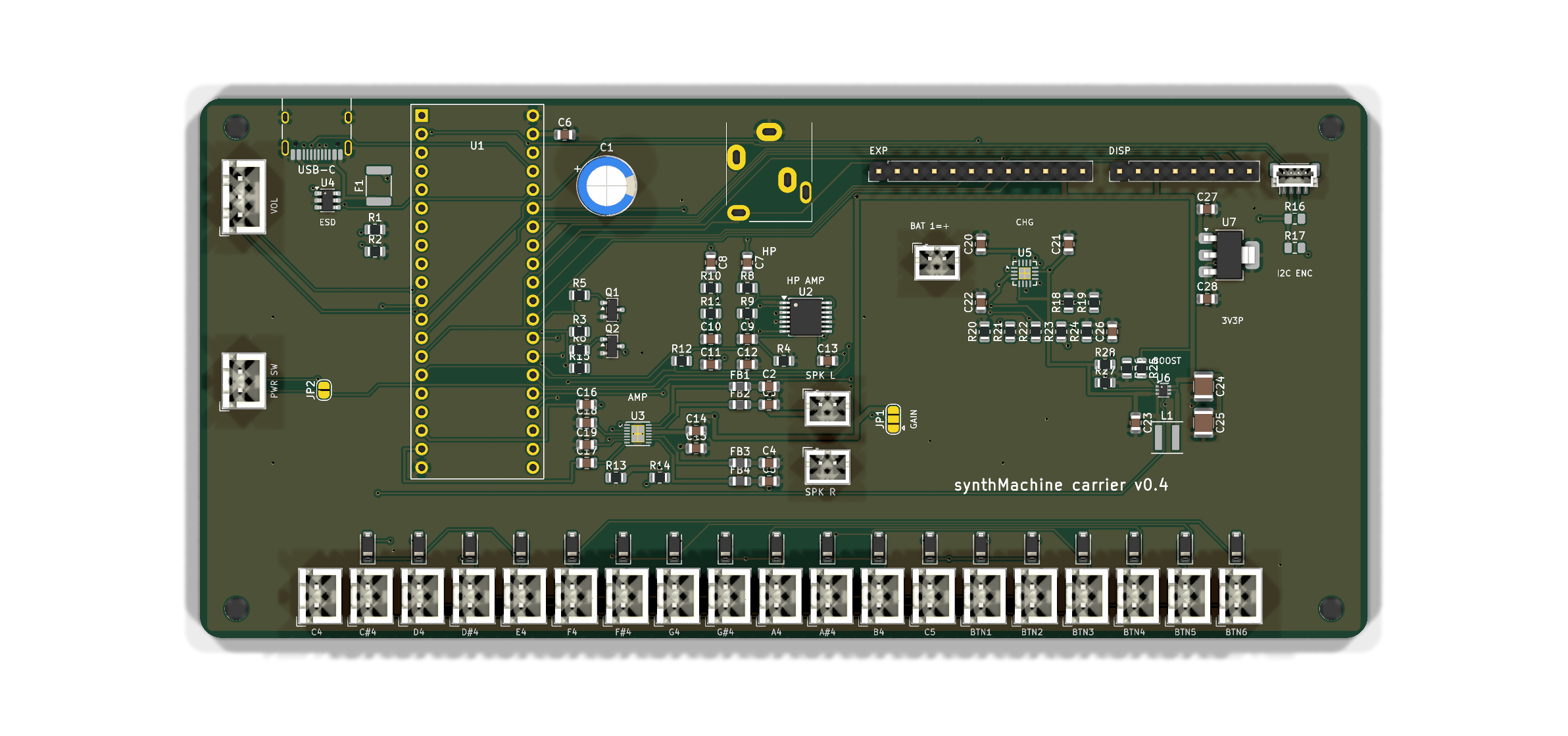
Second revision of the carrier. v0.3 in ../v0.3/ is the board that was fabricated in September 2026; v0.4 applies everything in ../NEXTREVISION.md and adds onboard battery power.
Synth machine is an open-source printed circuit board by zachtemkin, from the zachtemkin/synth-machine-libDaisy repository on GitHub. It is a 2-layer board of 160 × 74 mm with 123 parts on 94 nets, routed with 1,168 tracks and 118 vias.
It is built around the MAX98306ETD+T, BQ24074RGTR and USBLC6-2SC6, with the 1N4148W among its other parts. Its parts include 28 capacitors, 27 resistors, 19 switches, 18 diodes and 10 connectors. It belongs with the audio and music boards of this library.
Second revision of the carrier. v0.3 in ../v0.3/ is the board that was
fabricated in September 2026; v0.4 applies everything in ../NEXT_REVISION.md
and adds onboard battery power. It is a new outline: 160 x 74 mm landscape
instead of 100 x 100, with all 19 key headers in one row along the bottom
edge in panel order. The USB-C, the Seed's own USB and the headphone jack
still share the top edge.
Change
Parts
Why
One row of key headers
K1..K19 along the bottom at 7 mm pitch, diode above each, name below
Every button lead is the same length and points the same way. The headers are rotated so the row is 132 mm wide and the corners stay free for mounting holes.
Battery power
J17 JST-PH cell, U5 BQ24074 charger with power path, U6 TPS61023 5 V boost, J16 power-switch header, JP2 always-on jumper
Runs from a single LiPo, charges from the USB-C, and runs from USB while charging. See the power section below.
Plug detect reaches 3V3
Q1 is a 2N7002 MOSFET
The v0.3 BJT clamped HP_DET at 0.8 V so D13 never saw a plug. No jumper, no HP_DET=adc.
Firmware mute on its own transistor
Q2 2N7002, R6 gate, R15 pull-up; MUTE on D0
Muted at reset, in DFU and after a crash; firmware drives D0 low to run. Wired-OR with Q1.
I2C for encoders
J15 STEMMA QT (top-entry) on I2C1 (D11 SCL, D12 SDA) at the top right; R16/R17 pull-ups DNP
For the seesaw rotary-encoder breakouts; the cable leaves upward toward the panel.
The four bank controls are seesaw rotary encoders on J15. Their old ADC pins go to the expansion header.
USB ESD, SMD fuse
U4 USBLC6-2SC6, F1 1812 PTC on the USB input
Data lines were unprotected; the radial fuse collided with the Seed.
USB-C receptacle
J1 is the HRO TYPE-C-31-M-12 (LCSC C165948)
Same land pattern and body depth as v0.3's GCT USB4105, which went out of stock. A JLCPCB basic part.
Peripheral 3.3 V rail
U7 AP7361C-33 (SOT-223, 1 A) from +5V, C27/C28
Feeds the encoders, the display and the expansion header's 3V3 pin, so the Seed's regulator carries only the Seed, the headphone amp and pull-ups.
Assembly-ready BOM
every part has an MPN or LCSC number
fab.sh writes pcbway_bom.csv / pcbway_cpl.csv.
Only the volume pot header remains (A0). The four bank controls are I2C
rotary encoders on J15, chained over STEMMA QT. The firmware profile
HW=carrier4 reads A0 only and leaves the bank inputs alone until the
encoder support exists.
Power
text
USB-C J1 -> F1 2.5 A PTC -> VUSB -> U5 BQ24074 IN
                                    U5 BAT  <-> J17 cell (+ C22)
                                    U5 OUT   -> VSYS (4.4 V on USB, else the cell)
VSYS -> L1 1 uH / U6 TPS61023 -> +5V (5.1 V) -> Seed VIN, speaker amp, J8/J9 5V pins
                                       +5V -> U7 AP7361C-33 -> 3V3P -> J15 encoders, J9 display, J8 3V3
Charger. EN2 high and EN1 low select the resistor-programmed input
limit: R19 1.1k gives 1.5 A, and the charger's input-voltage loop backs off
automatically on a weak USB port. R18 1.8k sets 0.5 A fast charge, which is
0.25 C for a 2000 mAh cell and keeps the linear charger under 0.7 W. TMR and
ITERM are left open for the default 30 min / 5 h safety timers and 10 %
termination. CE is tied low, TS has the 10k that the part needs when there
is no pack thermistor. The system runs from OUT while the cell charges, and
the cell supplements USB on peaks.
Boost. The TPS61023 makes 5.1 V from VSYS (750k/100k on a 0.6 V
reference). It carries the whole load on USB as well as on battery, which is
fine: from the charger's 4.4 V it is barely working. From a 3.3 V cell it
delivers about 1.5 A continuous with the 470 uF C1 covering the amp's
peaks. Inductor per TI's table (Coilcraft XEL4030-102ME); XGL4030-102MEC is
the LCSC-stocked equivalent.
Switch. J16 takes a panel SPST. Closed, it pulls the boost's EN up to
VSYS through R28; open, R27 holds it low and everything downstream of the
boost is off, while the charger keeps charging. The EN pin draws nothing,
so any small switch works. J16 sits on the left edge at mid-height with JP2
beside it to bridge the switch on a bench board; the two enable lines run
across the board to the boost, which is fine for a pull-up-and-pin signal.
Firmware signals. A10 reads VBAT/2 (R23/R24, 0 to 2.1 V). A5 reads
~CHG (low = charging) and A11 reads ~PGOOD (low = USB present), both
open-drain with 100k pull-ups. Nothing in the firmware uses them yet.
Cell. Single-cell LiPo on J17, pin 1 = +. Use a protected cell (the
Adafruit and SparkFun packs are); there is no protection on the board.
2000 mAh or more suits the speakers, which can pull over 1 A at volume.
Note. The Seed's own USB port powers only the Seed; it cannot charge
the cell or run the amp. That was already true on v0.3.
Regenerate, route, fab
Same pipeline as v0.3, run from this directory:
bash
KICAD_PY=/Applications/KiCad/KiCad.app/Contents/Frameworks/Python.framework/Versions/Current/bin/python3
$KICAD_PY hardware/v0.4/gen_kicad.py                       # schematic + placed PCB
$KICAD_PY hardware/v0.4/route.py --java <java25> --jar freerouting-2.4.1.jar
$KICAD_PY hardware/v0.4/route.py --pours-only              # rebuild just the GND pours
sh hardware/v0.4/fab.sh                                    # Gerbers, BOMs, CPLs, test print
Freerouting 2.4.1 needs Java 25. Neither is installed system-wide on the
Mac; a portable Temurin JRE from adoptium.net and the jar from the Freerouting
GitHub releases page were used, and both can live anywhere. PREROUTES in
the generator carries the audio paths, the MAX98306 fan-out and short stubs
off the boost converter's 0.5 mm pitch pins, which the autorouter cannot reach
with power-width tracks on its own.
Pin map (what the firmware profile HW=carrier4 expects)
Seed pin
Use
D0
MUTE: high = speakers muted (default via R15), low = run
D1..D3
matrix rows
D4..D9
matrix columns
D10
C4 key
D11, D12
I2C1 SCL, SDA (STEMMA QT)
D13
HP_DET, high = headphones plugged in
D14
HP_MUTE, headphone amp ~MUTE, low = muted
A0
volume pot
A1, A2, A4, A9
spare, on J8 (the old bank pot inputs)
A3, A7, A8
SPI1 MOSI, SCK, NSS (display)
A5
~CHG from the charger, low = charging
A6
spare, on J8 (seesaw INT candidate)
A10
battery voltage / 2
A11
~PGOOD from the charger, low = USB present
D26, D27
display D/C, RST
D29, D30
USB-C data (MIDI)
Headers
Ref
What
Pins
K1..K19
keys, JST-XH 2-pin, bottom row in panel order
row / diode (any way round)
J10
volume pot, JST-XH 3-pin, left edge below the USB-C
3V3A, wiper, GND
J5, J6
speakers, JST-PH
+ / -
J17
battery, JST-PH
1 = +, 2 = GND
J16
power switch, JST-XH 2-pin, left edge mid-height (JP2 beside it bridges it)
fab.sh writes fab/pcbway_bom.csv with an item per line: designators,
quantity, manufacturer part number, LCSC number, value, package and whether it
is SMD or through-hole. fab/pcbway_cpl.csv has both sides. Upload the
Gerber zip, the BOM and the CPL; on the quote, tick at least J1 (USB-C), the
19 K headers, J10, J5/J6, J16, J17 and J15 for placement. The Seed
sockets, C1 and the jack can go in the same job or be hand-fitted.
Ordering with assembly (JLCPCB)
fab/jlcpcb_bom.csv and fab/jlcpcb_cpl.csv carry every part with an LCSC
number, which is all of the SMD parts and the JST connectors: the 19 key
headers, the volume and switch headers (JST XH originals, C158012 /
C144394) and the speaker and battery sockets (JST PH, C131337). Choose
standard assembly, not economic: economic is SMD-only and drops the
through-hole connectors. Still hand-fitted afterwards: the two Seed sockets,
the two expansion/display sockets, the headphone jack and C1, which are on
the Digi-Key list. The DNP pull-ups are excluded automatically.
Design review notes (v0.4 quality pass)
Things checked after the layout settled, and what was changed or accepted:
Current paths. Every net that carries real current was audited for
width: VBUS/VUSB/VBAT/VSYS 0.4 mm, +5V and the filtered speaker lines
0.6 mm, with 0.5 mm-drill vias. The only narrow copper left is the
unavoidable necks onto fine-pitch pads: 0.3 mm for less than 1 mm at the
boost's VIN/SW/VOUT/GND pins (0.35 mm pads, 0.5 mm pitch) and 0.2 mm for
about 1 mm at the amp's PVDD and speaker pins (0.4 mm pitch). The amp's
two PVDD pins are joined right off the pads into one 0.5 mm feed. The
boost's input and output capacitors sit at its pins with 0.6 mm copper.
Power switch really switches off. The TPS61023 has true input-to-output
disconnect in shutdown, so with EN low nothing reaches the Seed's VIN.
Bulk capacitor on the boost. The 470 uF electrolytic on +5V is inside
the TPS61023's stated 4 to 1000 uF effective output range.
Boost thermals. SOT-563 is about 120 to 140 K/W. At 1 A out from a
3.3 V cell the part dissipates about 0.5 W, so it runs warm (60 K rise)
but within limits; the amp's 2 A peaks are brief. Keep the ground pour
under it. If a future revision needs more headroom, the TPS61088 in a
QFN is the drop-in class.
Seed 3V3 budget. Solved with a separate rail: the Seed's regulator
feeds only the Seed, the headphone amp and the pull-ups (tens of
milliamps). The encoders, display and expansion header run from U7, a
1 A SOT-223 LDO on the +5V rail (3V3P). At 300 mA it dissipates about
0.55 W, a 30 K rise on its ground tab and pour. On battery that rail is
boost-then-LDO, roughly 60 % efficient, about 20 mA of extra cell current
at typical loads. The headphone amp stays on the Seed's quieter rail.
USB-C current. The CC pull-downs advertise a sink but the firmware does
not read the source's advertisement, so the charger's 1.5 A input limit
applies to any port; the charger's VIN-DPM loop throttles rather than
crashes a 500 mA port. A CC ADC read would let firmware lower ILIM later.
Battery divider on the ADC. 100k/100k is a 50k source impedance, high
for the STM32 ADC's sampling time; the 100 nF across the bottom resistor
is what makes the reading settle. Do not drop it.
Reverse cell. No reverse-polarity protection on J17 by design (a diode
would cost the charger its regulation). The polarity check below is the
protection.
Quiescent when off. Charger from the cell, boost leakage and the sense
divider add up to about 25 uA, years on any usable cell.
Check before ordering
J17 polarity against the cell you will use: pin 1 is + here, and the
silkscreen says so. A reversed cell destroys the charger.
J15 pin 1 (GND) is the pad nearest the board's right edge; check it
against the cable's black wire before plugging in an encoder board.
Q1/Q2 pinout: KiCad's Q_NMOS_GSD is gate 1, source 2, drain 3, the
2N7002's SOT-23 order. Check the LCSC part's datasheet agrees.
U5 thermal pad has vias to the ground pour; make sure the assembler's
stencil does not flood it.
Enclosure: the outline changed. The top edge still carries all three
ports at the same spacing from the left edge as v0.3, but the board is
60 mm wider and 26 mm shorter, and the mounting holes moved. The headphone
jack's nose now stands 1.5 mm proud of the edge instead of flush.
F1 and L1 look unpopulated in the render only because this KiCad
install has no 3D models for the 1812 fuse and the XxL4030 inductor
footprints. Both are in the BOM and the placement file.
Second revision of the carrier. v0.3 in ../v0.3/ is the board that was fabricated in September 2026; v0.4 applies everything in ../NEXTREVISION.md and adds onboard battery power.
Open hardware for the Semtronik Link devices: ESP32-S3 base board, interface modules and enclosure. KiCad and Fusion sources, CERN-OHL-S v2.
115 parts
Questions
How big is the Synth machine PCB?
It measures 160 × 74 mm and has 2 copper layers, 1.6 mm thick.
What parts does the Synth machine use?
123 parts, built around the MAX98306ETD+T, BQ24074RGTR, USBLC6-2SC6 and 1N4148W. The full list of its parts is on this page, with links to each part's symbol and footprint where PCBKit's library has them.
Where can I download the Synth machine KiCad files?
From the zachtemkin/synth-machine-libDaisy repository on GitHub, at the commit this page was made from: the board is hardware/v0.4/synth_machine.kicad_pcb and its schematic hardware/v0.3/synth_machine.kicad_sch. PCBKit opens the board in the browser, with nothing to install.
Can I use the Synth machine design in my own project?
Its repository states no licence, so its author keeps all rights: ask zachtemkin before reusing the design.