2 layers358.8 × 125.1 mm

 yskoht/pakbd-device
My keyboard
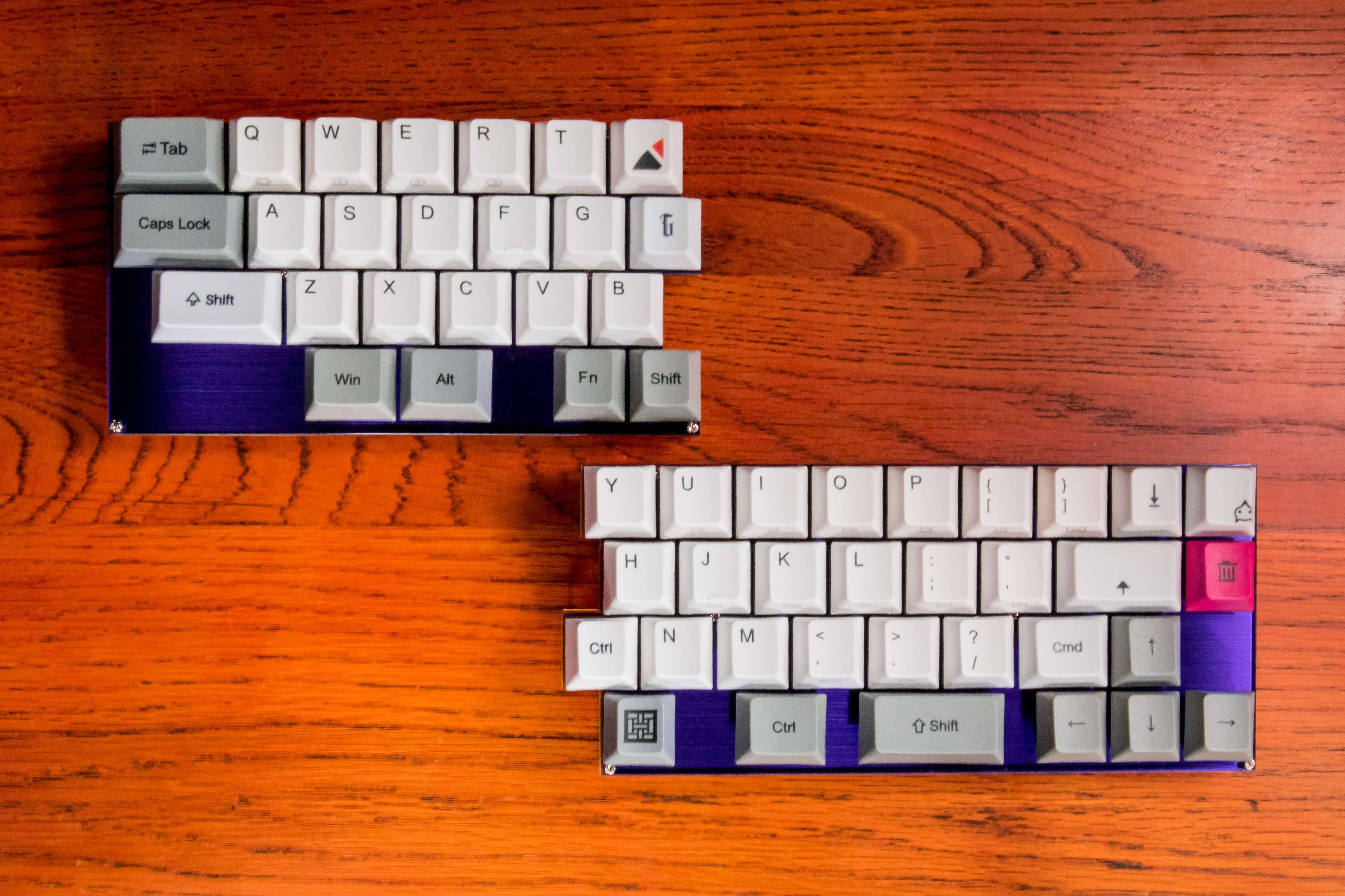
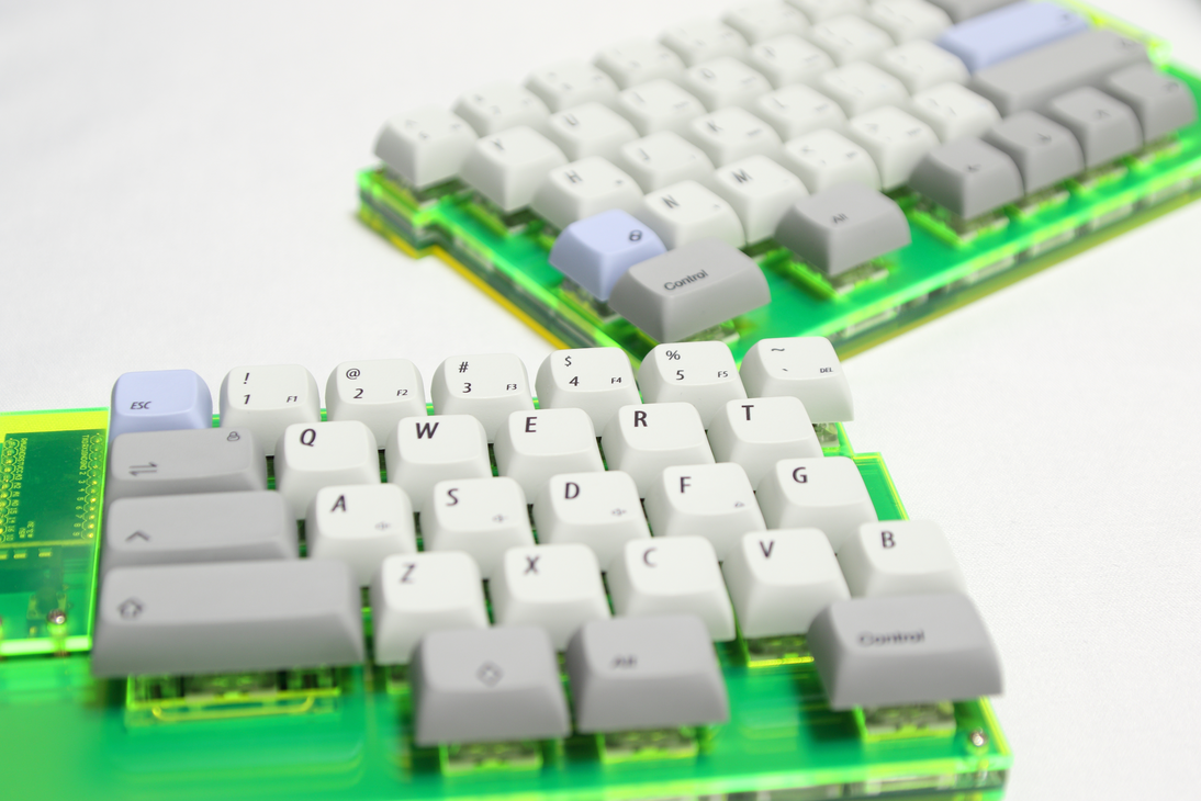
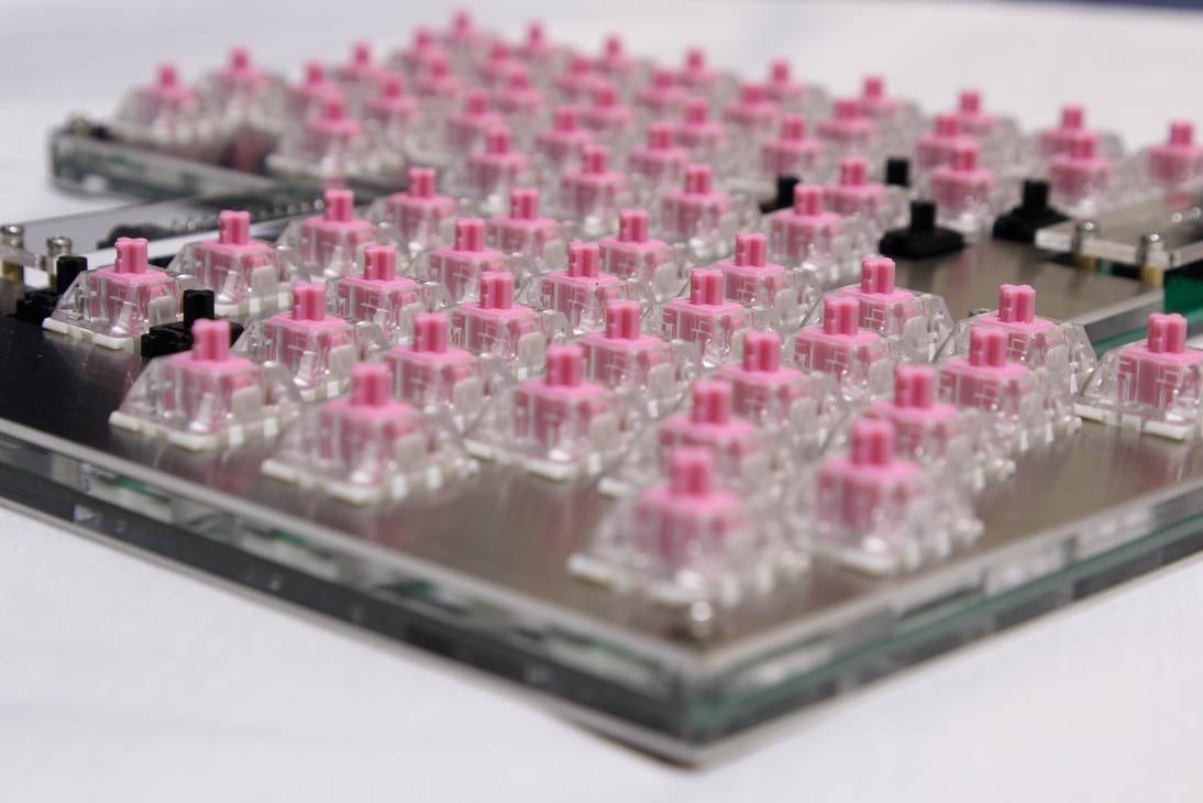
Pakbd is an open-source printed circuit board by yskoht, from the yskoht/pakbd-device repository on GitHub, published under the MIT licence. It is a 2-layer board of 368.3 × 101.3 mm with 190 parts on 114 nets, routed with 1,033 tracks and 268 vias.
Its parts include 70 diodes, 70 switches, 2 ICs and 2 connectors. It belongs with the keyboards and input boards and the AVR (ATmega, ATtiny) boards of this library.


This software is released under the MIT License, see LICENSE.
| Qty | Value | Footprint | References |
|---|---|---|---|
| 70 | DIODE | Diode_SMD:D_1206_3216Metric_Pad1.42x1.75mm_HandSolder | D0, D1, D2, D10, D11, D12, D13, D14, D15, D16, D17, D18, D19, D20, D21, D22 +54 |
| 61 | SW_Push | CPG151101S11:CPG151101S11_1.00u_PCB | SW0, SW1, SW2, SW10, SW11, SW12, SW13, SW15, SW16, SW17, SW18, SW19, SW20, SW22, SW23, SW24 +45 |
| 32 | MountingHole_3.2mm_M3 | MountingHole:MountingHole_3.2mm_M3 | cr00, cr01, cr02, cr03, cr04, cr05, cr06, cr10, cr11, cr12, cr13, cr14, cr15, cr16, cr17, cr18 +16 |
| 8 | Jumper | Jumper:SolderJumper-2_P1.3mm_Open_Pad1.0x1.5mm | JP_da0, JP_da1, JP_db0, JP_db1, JP_xa0, JP_xa1, JP_xb0, JP_xb1 |
| 5 | SW_Push | CPG151101S11:CPG151101S11_1.25u_PCB | SW27, SW28, SW62, SW65, SW66 |
| 4 | R | Resistor_SMD:R_1206_3216Metric_Pad1.42x1.75mm_HandSolder | R_data0, R_data1, R_xdata0, R_xdata1 |
| 3 | SW_Push | CPG151101S11:CPG151101S11_1.75u_PCB | SW14, SW21, SW54 |
| 2 | MJ-4PP-9 | MJ-4PP-9:MJ-4PP-9 | J0, J1 |
| 2 | ProMicro | promicro:ProMicro | U0, U1 |
| 2 | SW_Push | Button_Switch_THT:SW_Tactile_Straight_KSA0Axx1LFTR | SW_r0, SW_r1 |
| 1 | SW_Push | CPG151101S11:CPG151101S11_1.50u_PCB | SW7 |

PCBench/PCBench
resolution = [0.5, 0.5] pcbfolder = '../PCBs/' pcbnames = ["1Bitsy1bitsy"] iters = 30 env = PCBRoutingEnv(resolution=resolution, pcbfolder=pcbfolder, pcbnames=pcbnames) obs, info = env.reset() for in range(iters): act =…

OnionDAO-git/oniondao-badge
An open-source, hacker-conference-style electronic badge built around the ESP32-S3-WROOM-1-N8R8 (8 MB flash + 8 MB Octal PSRAM), with swappable RF / audio / storage modules, an e-paper (or TFT) display socket, a secure…


olin-electric-motorsports/MKV-Boards
Repository for all OEM MKV PCB Projects

Secant1006/Audician-32-Plus-Replica
An ISA Sound Card Based on Yamaha YMF71x (OPL3-SAx) Chip


krunchiekrunch/krunchboard-90
A custom 75% (84+4+1) sandwich-mount ANSI mechanical keyboard powered by a Raspberry Pi Pico with KMK
It measures 368.3 × 101.3 mm and has 2 copper layers, 1.6 mm thick.
190 parts. The full list of its parts is on this page, with links to each part's symbol and footprint where PCBKit's library has them.
From the yskoht/pakbd-device repository on GitHub, at the commit this page was made from: the board is rev1/pcb/pakbd/pakbd.kicad_pcb. PCBKit opens the board in the browser, with nothing to install.
Its repository publishes it under the MIT licence: you may reuse it on that licence's terms (keep the author's notice, and for a copyleft licence share your changes alike).
