2 layers368.3 × 101.3 mm

 yskoht/pakbd-device
My keyboard
Pakbd is an open-source printed circuit board by yskoht, from the yskoht/pakbd-device repository on GitHub, published under the MIT licence. It is a 2-layer board of 358.8 × 125.1 mm with 213 parts on 122 nets, routed with 1,490 tracks and 254 vias.
Its parts include 79 switches, 78 diodes, 4 connectors and 2 ICs. It belongs with the keyboards and input boards and the AVR (ATmega, ATtiny) boards of this library.
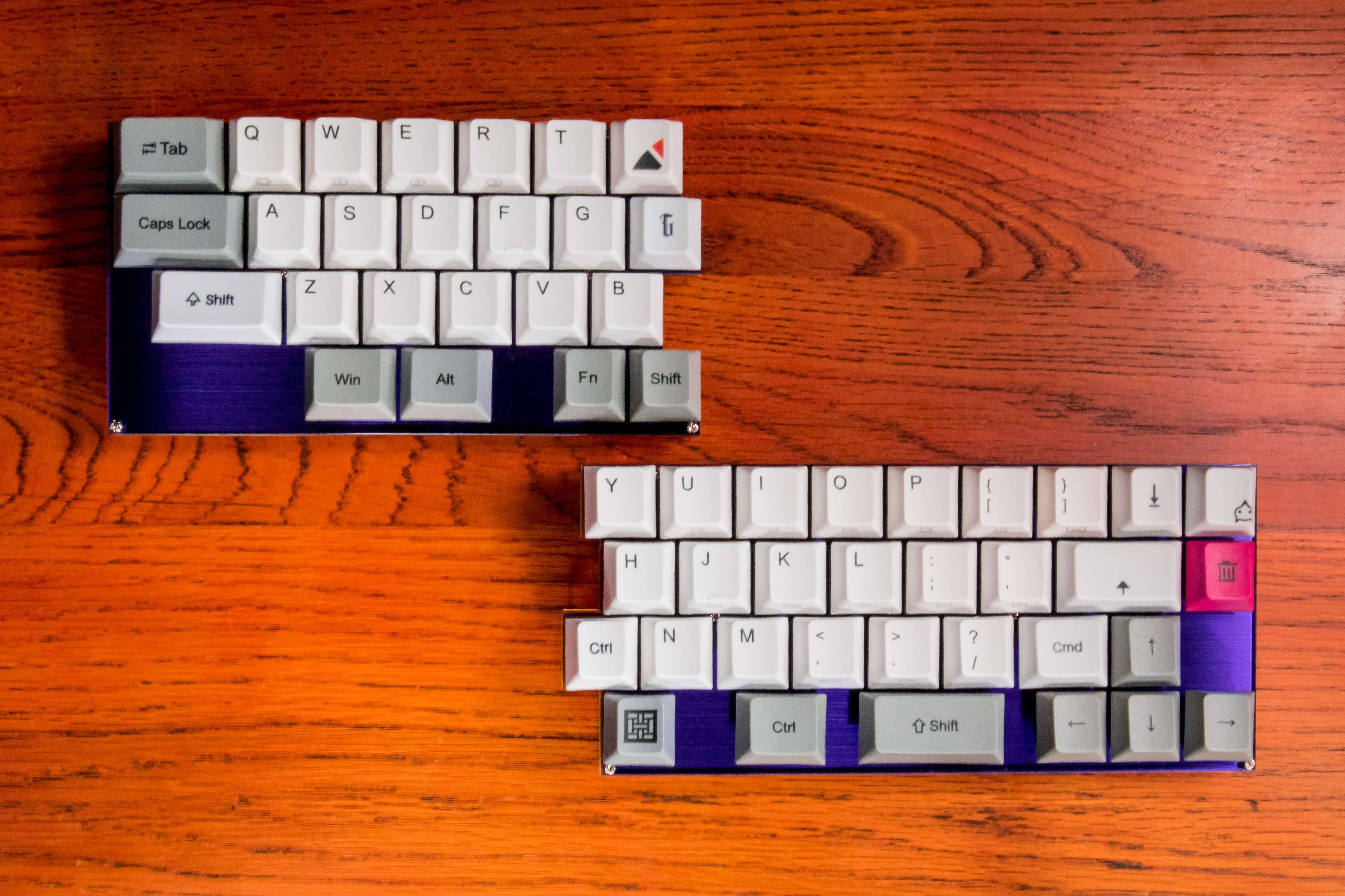


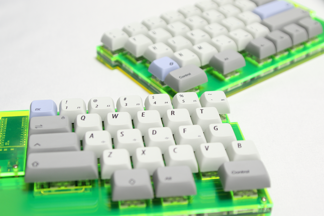
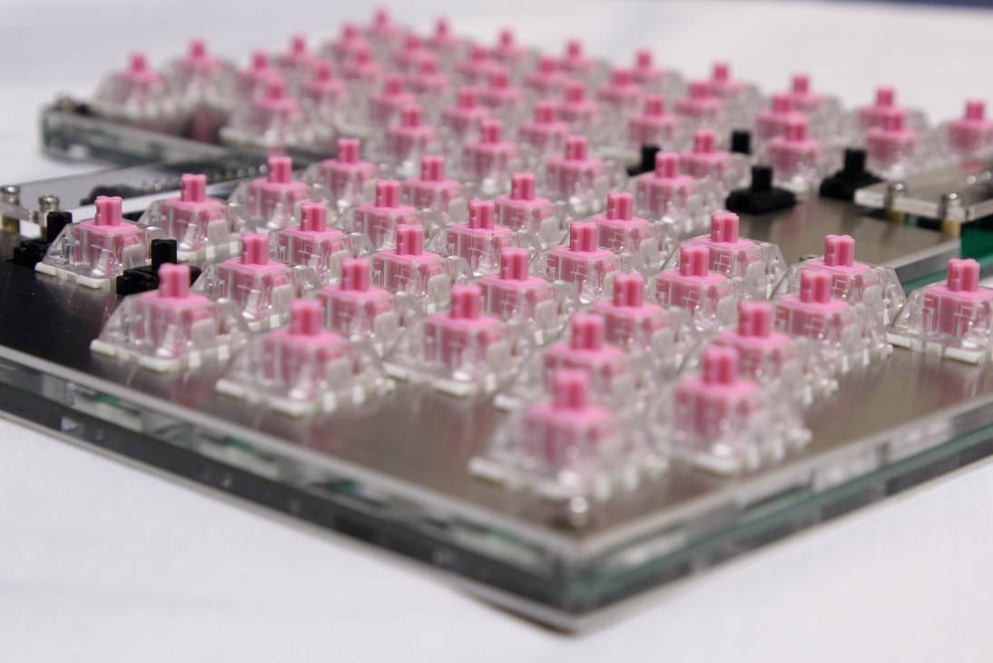
This software is released under the MIT License, see LICENSE.
| Qty | Value | Footprint | References |
|---|---|---|---|
| 78 | DIODE | Diode_SMD:D_1206_3216Metric_Pad1.42x1.75mm_HandSolder | D0, D1, D2, D10, D11, D12, D13, D14, D15, D16, D17, D18, D19, D20, D21, D22 +62 |
| 68 | SW_Push | CPG151101S11:CPG151101S11_1.00u_PCB | SW0, SW1, SW2, SW10, SW12, SW13, SW14, SW15, SW16, SW18, SW19, SW20, SW21, SW22, SW24, SW25 +52 |
| 8 | Jumper | Jumper:SolderJumper-2_P1.3mm_Open_Pad1.0x1.5mm | JP_da0, JP_da1, JP_db0, JP_db1, JP_xa0, JP_xa1, JP_xb0, JP_xb1 |
| 4 | MJ-4PP-9 | MJ-4PP-9:MJ-4PP-9 | J0, J1, J2, J3 |
| 4 | R | Resistor_SMD:R_1206_3216Metric_Pad1.42x1.75mm_HandSolder | R_data0, R_data1, R_xdata0, R_xdata1 |
| 4 | SW_Push | CPG151101S11:CPG151101S11_2.25u_PCB | SW23, SW31, SW64, SW72 |
| 3 | SW_Push | CPG151101S11:CPG151101S11_1.25u_PCB | SW29, SW30, SW73 |
| 2 | ProMicro | ProMicro:ProMicro | U0, U1 |
| 2 | SW_Push | CPG151101S11:CPG151101S11_1.50u_PCB | SW11, SW57 |
| 2 | SW_Push | Button_Switch_THT:SW_Tactile_Straight_KSA0Axx1LFTR | SW_r0, SW_r1 |
| 1 | SW_Push | CPG151101S11:CPG151101S11_2.75u_PCB | SW71 |
| 1 | SW_Push | CPG151101S11:CPG151101S11_1.75u_PCB | SW17 |
The 177 most common of 213 parts.

neuroidss/FreeEEG32-beta
as FreeEEG32 plus alpha1.5 test passed, FreeEEG32 project changed to beta version


Tjeerdie/SPECTRE
Speeduino compatible engine control unit (ECU) based around black STM32F407VET6 board.

karnadii/marvelous65-split
65% keyboard staggered split wikth oled and encoder on both side

freeDSP/FreeDSP_Catamaran_AB
A mono contruction Differntial 1 Input 4 output ADAU1701 DSP board, 96kHz TDM8 interlink is available.


gohanda11/HEball
A split keyboard powered by Hall Effect (magnetic) switches with a trackball on the right half.

It measures 358.8 × 125.1 mm and has 2 copper layers, 1.6 mm thick.
213 parts. The full list of its parts is on this page, with links to each part's symbol and footprint where PCBKit's library has them.
From the yskoht/pakbd-device repository on GitHub, at the commit this page was made from: the board is rev2/pcb/pakbd/pakbd.kicad_pcb. PCBKit opens the board in the browser, with nothing to install.
Its repository publishes it under the MIT licence: you may reuse it on that licence's terms (keep the author's notice, and for a copyleft licence share your changes alike).
