8 layers115.3 × 25.3 mm
PROC091G
um-kiho/ti_radar
AWR6843AOP (Antenna-on-Package) 60GHz FMCW 레이더를 이용한 존재 감지(Presence Detection) 시스템입니다. 내장 ARM Cortex-R4F MCU + C674x DSP에서 신호 처리 및 존재 판정을 수행하고, UART로 결과를 출력합니다.
446 parts

 YikeStone/pereda-kbd1
Pereda is a custom wireless mechanical keyboard designed for Kailh Choc V1 switches.
Pereda choc is an open-source printed circuit board by YikeStone, from the YikeStone/pereda-kbd repository on GitHub. It is a 2-layer board of 148.9 × 97.5 mm with 51 parts on 44 nets, routed with 683 tracks and 88 vias.
It is built around the 1N4148W, PCM12SMTBR and M50-3930342. It belongs with the keyboards and input boards and the nRF52 and nRF5x boards of this library.


Pereda is a custom wireless mechanical keyboard designed for Kailh Choc V1 switches.
It has 46 keys, aggressive column stagger, and column splay. The key positions are designed around my finger length and natural finger-joint movement rather than a conventional keyboard layout.
Finished Product:
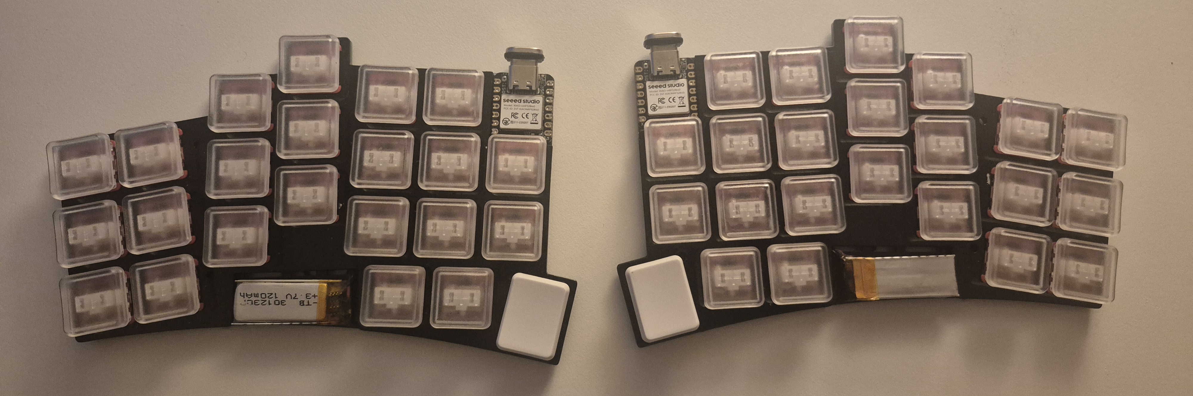
After soldering the XIAO nRF52840 module to the PCB, a battery pad on the underside of the XIAO remains accessible through the cutout in the PCB.
Solder the exposed battery pad on the XIAO to the corresponding battery pad on the PCB using a short wire.
The PCB is reversible, allowing the same PCB design to be used for either side.
Pereda uses ZMK firmware.
Ready-to-manufacture files are available under:
manufacturing/v0.2/
The BOM quantities are for one PCB/half.
common/ — custom symbols, footprints, and 3D modelsimages/ — project imagesmanufacturing/ — BOM, fabrication files, DXF, and CAD*.kicad_* — KiCad source filesv0.2 — functional prototype.
Inspired by the Corne keyboard by foostan.
See LICENSE.
| Qty | Value | Footprint | References |
|---|---|---|---|
| 23 | 1N4148WT | kbd:D_SOD-123-rev | D2, D10, D11, D12, D13, D14, D15, D16, D17, D18, D19, D20, D21, D22, D23, D24 +7 |
| 22 | SW_Push | kbd:Kailh_socket_PG1350_reversible_1u | rSW2, rSW3, rSW10, rSW11, rSW12, rSW13, rSW14, rSW15, rSW16, rSW17, rSW18, rSW19, rSW20, rSW21, rSW22, rSW23 +6 |
| 2 | SPDT | Button_Switch_SMD:SW_SPDT_PCM12 | rSMDSW1, SMDSW2 |
| 2 | XIAO-nRF52840-SMD | kbd:XIAO-nRF52840-SMD-kbd | rU6, U1 |
| 1 | Conn_01x03 | Connector_PinHeader_2.54mm:PinHeader_1x03_P2.54mm_Horizontal | rJ2 |
| 1 | SW_Push | kbd:Kailh_socket_PG1350_reversible_1.25u | rSW1 |
It measures 148.9 × 97.5 mm and has 2 copper layers, 1.6 mm thick.
51 parts, built around the 1N4148W, PCM12SMTBR and M50-3930342. The full list of its parts is on this page, with links to each part's symbol and footprint where PCBKit's library has them.
From the YikeStone/pereda-kbd repository on GitHub, at the commit this page was made from: the board is pereda-choc.kicad_pcb and its schematic common/left.kicad_sch. PCBKit opens the board in the browser, with nothing to install.
Its repository states no licence, so its author keeps all rights: ask YikeStone before reusing the design.
um-kiho/ti_radar
AWR6843AOP (Antenna-on-Package) 60GHz FMCW 레이더를 이용한 존재 감지(Presence Detection) 시스템입니다. 내장 ARM Cortex-R4F MCU + C674x DSP에서 신호 처리 및 존재 판정을 수행하고, UART로 결과를 출력합니다.

stephan-biomedical-engineer/Electroencephalogram
This project focuses on developing a wearable Electroencephalogram (EEG) device, integrating key concepts from Internet of Things (IoT) and embedded systems for biopotential acquisition.

ben5049/cm-carrier-hardware
Compact CM5 carrier board with an M.2 E-key connector and a 1000BASE-T1 Ethernet PHY, as well as other optional IO.

ben5049/Keyboard
Features: - Wireless - 900mAh battery - Bluetooth (nRF52) - ZMK - 4 Port USB hub - BLDC Knob for haptic feedback - Kailh Choc V1 switches

NilsEngelbach/air-quality-pcb
Seventh iteration: ESP8266 → ESP32-C3 (native USB, no UART bridge), fixes from the v6 design review, right-angle switches with longer actuators, a STEMMA QT port for optional sensors, and charge-status sensing.

fossasia/pslab-hardware
PSLab Hardware Design and Schematics https://pslab.io

pierrechevalier83/ferris
A low profile split keyboard designed to satisfy one single use case elegantly
