


4 layers72.7 × 88.7 mm
Optimus Hub
devisunofficial/Optimus-Hub
Optimus hub is a USB 2.0 hub which has USB Type-C upstream port and 6 downstream USB Type-A port and one TF-Card reader
76 parts

 yash-mehta13/4-Port-USB-Hub1
A KiCad 8 design for a self-powered 4-port USB hub board. The schematic names a Genesys Logic GL850G hub controller (IC1, value GL850G-HH), one upstream USB-A connector (J5), four downstream USB-A connectors (J1–J4), a…
USB Hub Port Extender is an open-source printed circuit board by yash-mehta13, from the yash-mehta13/4-Port-USB-Hub repository on GitHub. It is a 4-layer board of 55 × 65 mm with 54 parts on 46 nets, routed with 450 tracks and 45 vias.
It is built around the GL850G-HHY60 and ECS-120-18-4X-CKM. Its parts include 22 capacitors, 13 resistors, 6 connectors, 6 inductors and 4 ICs. It belongs with the interfaces and adapters boards of this library.
A KiCad 8 design for a self-powered 4-port USB hub board. The schematic names a Genesys Logic GL850G hub controller (IC1, value GL850G-HH), one upstream USB-A connector (J5), four downstream USB-A connectors (J1–J4), a DC barrel-jack power input (CN1), per-port polyfuses, ferrite beads and bulk capacitors, SRV05-4 ESD arrays, a 12 MHz crystal, and a gang-mode LED.
Status: design in progress — not ready for fabrication. A source-level audit (see docs/validation-report.md) found several connectivity defects in the schematic and PCB, including a net that ties USB port 2's D− line to the 5 V rail, swapped D+/D− on port 1, an unconnected reset input, and a hub-controller symbol that is actually a Microchip MCP23017 I/O-expander symbol. No board has been fabricated or tested, no KiCad ERC/DRC has been run (KiCad was not available in the audit environment), and no USB compliance claim is made. Details in Known issues.
Purpose · Images · Design summary · Specifications · Opening the project · Libraries and models · Validation status · Known issues · BOM · Fabrication · Safety · Docs · License · Roadmap · Contributing
A USB hub turns one host USB port into several. This project is a learning/portfolio hardware design that implements a hub on a custom 4-layer board using a single-chip hub controller, with an external 5 V barrel-jack supply so downstream ports are not powered solely from the host. See docs/project-overview.md.
All images are real KiCad screenshots of this design (taken 2026-01-22/23, i.e. intermediate states of the design, not a verified final revision). There is no photograph of a fabricated or assembled board in this repository.
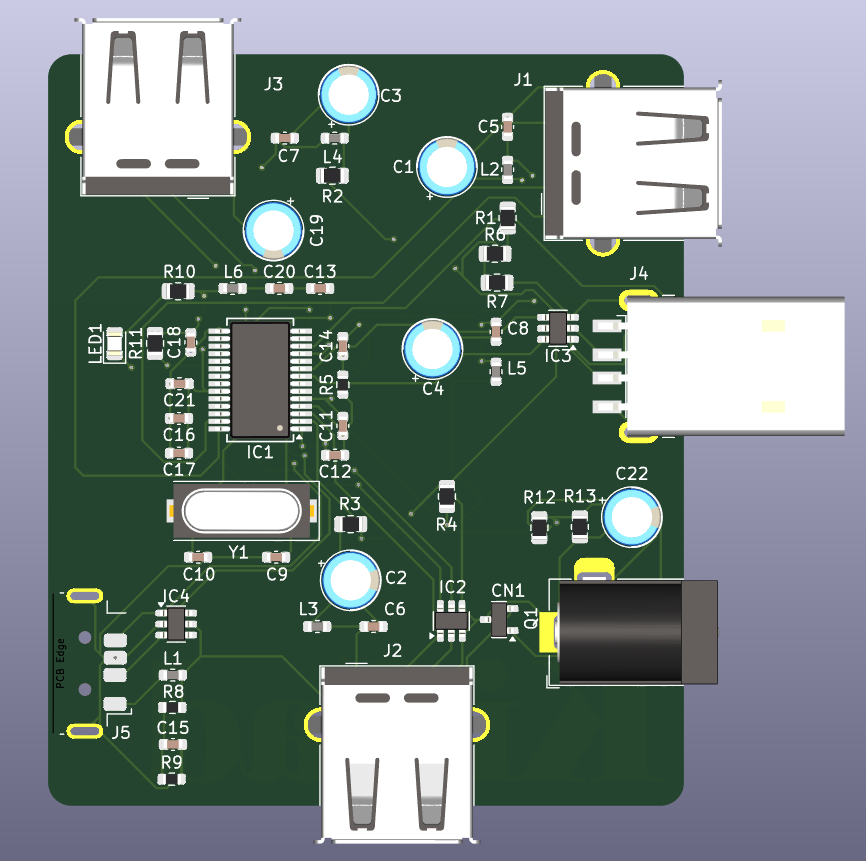 | 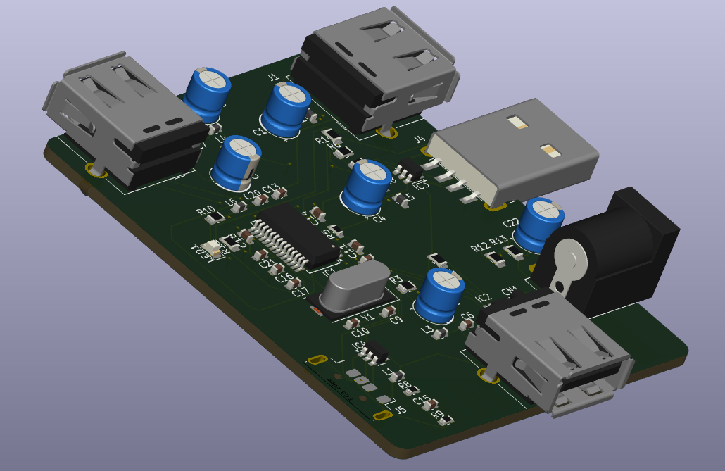 |
| 3D viewer, top view: five USB-A connectors, DC jack, HC-49 crystal, SSOP-28 hub IC. | 3D viewer, perspective: through-hole radial bulk capacitors, mixed horizontal connector styles. |
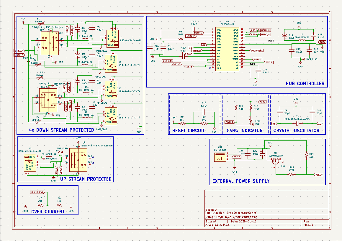 Single-sheet schematic (A4, dated 2026-01-12): downstream ports, hub controller, reset, gang indicator, crystal, upstream, overcurrent network and external power.
| Image | Content |
|---|---|
| pcb-layout-all-layers.png | PCB editor, all layers visible, board with zone fills |
| pcb-layout-bottom-active.png | PCB editor, back copper highlighted (large "KiCad" logo text is on B.Cu) |
| schematic-downstream-and-controller.png | Downstream ports J1–J4 with IC2/IC3 and hub controller IC1 |
| schematic-upstream-and-overcurrent.png | Upstream J5/IC4 and the overcurrent divider (R6/R7) |
| schematic-reset-gang-crystal-power.png | Reset network, gang LED, crystal, external power and Q1 |
IC1, value GL850G-HH, 28-pin SSOP footprint. Genesys Logic is the manufacturer implied by the value; the official datasheet could not be retrieved during the audit, so the pin map is not verified (see D1 in circuit-design).J5 (Type-A) → IC4 SRV05-4 → hub pins 25/26 (USB0_N/USB0_P). Upstream VBUS passes through ferrite L1 to net +5V.J1–J4 ↔ USB1–USB4 pairs on hub pins 27/28, 2/3, 8/9, 11/12; ESD arrays IC2 (ports 1–2) and IC3 (ports 3–4). Each port has a 500 mA-labelled polyfuse (R1–R4), ferrite bead (L2–L5), 100 µF + 0.1 µF.CN1 → rail VCC; Q1 (P-MOSFET) links +5V (host VBUS) and VCC. Hub analog rail AVDD is DVDD through ferrite L6.Y1 12 MHz, 2×33 pF.F.Cu, In1.Cu=GND zone, In2.Cu=+5V zone, B.Cu), 1.6 mm. 45 vias (0.6/0.3 mm), all tracks 0.2 mm.Only values read from the design files are listed.
| Item | Value | Source |
|---|---|---|
| Hub controller (per value field) | GL850G-HH, SSOP-28 footprint | schematic/PCB |
| Downstream / upstream connectors | 4 / 1 USB Type-A | schematic |
| Crystal | 12 MHz, 18 pF load (library description), 2×33 pF | schematic + library |
| Port polyfuses | value labelled 500 mA (part unspecified) | schematic |
| ESD arrays | 3× SRV05-4 | schematic |
| Board size | 55 × 65 mm | PCB Edge.Cuts |
| Layers / thickness | 4 / 1.6 mm (stackup in file; see caveats) | PCB |
| Net class | USD_diff: 0.2 mm width, 0.15 mm gap (applies to USB*) | project settings |
| Supply voltage, current budget, USB speed | not specified in the design | — |
USB speed is not asserted here: the supported speeds must be taken from the controller datasheet once the part is confirmed, and compliance has not been tested.
20231120, PCB format 20240108). KiCad 7 cannot open them.USB Hub Port Extender.kicad_pro.${KICAD8_3DMODEL_DIR} 3D models) must be installed. The schematic embeds its symbols; footprints are resolved from KiCad's stock libraries.The root holds SnapEDA-style library downloads: ECS-120-18-4X-CKM, MCP23017-E_SS, PMV20EN (.kicad_sym, footprints, .step, .zip). The current design instantiates none of their footprints, and the repo has no sym-lib-table/fp-lib-table. Only the ECS-120-18-4X-CKM and MCP23017-E_SS symbols are embedded in the schematic (the latter wrongly, as IC1). See docs/licensing-and-attribution.md and circuit-design.
| Check | Status |
|---|---|
| KiCad ERC | Not run (KiCad 8 / kicad-cli unavailable) |
| KiCad DRC | Not run |
| Schematic ↔ PCB net comparison | Run with tools/audit_netlist.py (independent script): one difference (J1 pin 5) |
| Gerber / drill / BOM / STEP export | Not run |
| Physical build, enumeration, USB compliance, ESD, thermal | Not done |
Full list with evidence: docs/validation-report.md and docs/circuit-design.md.
USB2_N: global label USB2_N sits on the VCC distribution wire; the PCB carries the same merged net. J2 pin 2 (D−), IC1 pins 2 and 23, SRV05-4 pins, Q1, CN1 pin 1 and all four polyfuse inputs share one net.J1 pin 2 (D−) is on USB1_P, pin 3 (D+) on USB1_N; J2–J5 are wired D−→_N.IC1 symbol is an MCP23017: pin names (GPA*, SCL, SDA…) and SnapEDA properties belong to an I²C I/O expander.RESET# not connected to the reset RC network (R8/R9/C15).OVCURR1# (R6/R7) vs OVCURR#1 (IC1 pin 21).J1 pin 5: unconnected in schematic, GND in PCB.USB4); impedance unverified.docs/bill-of-materials.csv – 54 parts grouped by value, matching all 54 PCB footprints. Most manufacturer part numbers are unresolved (the design stores generic values only); no sourcing links or prices are invented.
Summarised in docs/fabrication-guide.md. Do not order boards until the defects above are fixed, ERC/DRC are clean or justified, the fabricator's capabilities and stackup are agreed, and the impedance question is resolved.
Unprotected tests of an unvalidated design can short VBUS to data lines or back-feed a host. Read docs/safety-and-limitations.md and docs/hardware-validation.md before powering any assembled board.
| Document | Purpose |
|---|---|
| project-overview | scope, artifacts, status |
| circuit-design | schematic walkthrough and defects |
| pcb-layout-review | layers, routing, USB/power concerns |
| bill-of-materials.csv | components |
| fabrication-guide | outputs and reproduction steps |
| validation-report | what was and wasn't run |
| hardware-validation | bench checklist (all unchecked) |
| safety-and-limitations | risks |
| troubleshooting | symptoms → causes |
| decisions-and-roadmap | design decisions and ideas |
| licensing-and-attribution | license state |
| docs/reports/ | script-generated netlists/statistics |
No LICENSE file exists, so no open-source permissions are granted by default; the owner must choose a license. Third-party library content (SnapEDA downloads, KiCad stock libraries) is covered in docs/licensing-and-attribution.md. Author: yash-mehta13.
See docs/decisions-and-roadmap.md. Add a real board photograph and bench-test report once hardware exists.
See CONTRIBUTING.md.
| Qty | Value | Footprint | References |
|---|---|---|---|
| 12 | 0.1uF | Capacitor_SMD:C_0603_1608Metric | C5, C6, C7, C8, C11, C12, C13, C15, C17, C18, C20, C21 |
| 6 | FB-0603-2A | Inductor_SMD:L_0603_1608Metric | L1, L2, L3, L4, L5, L6 |
| 5 | 100uF | Capacitor_THT:CP_Radial_D5.0mm_P2.00mm | C1, C2, C3, C4, C22 |
| 4 | 500mA | Resistor_SMD:R_0805_2012Metric | R1, R2, R3, R4 |
| 3 | SRV05-4 - ESD Protection | Package_TO_SOT_SMD:SOT-23-6 | IC2, IC3, IC4 |
| 3 | USB-A-S-X-X-TH | Connector_USB:USB_A_Molex_67643_Horizontal | J1, J2, J3 |
| 2 | 1uF | Capacitor_SMD:C_0603_1608Metric | C14, C16 |
| 2 | 33pF | Capacitor_SMD:C_0603_1608Metric | C9, C10 |
| 2 | 470R | Resistor_SMD:R_0805_2012Metric | R10, R12 |
| 1 | 100k | Resistor_SMD:R_0805_2012Metric | R11 |
| 1 | 10k | Resistor_SMD:R_0805_2012Metric | R6 |
| 1 | 10k | Resistor_SMD:R_0603_1608Metric | R8 |
| 1 | 10uF | Capacitor_THT:CP_Radial_D5.0mm_P2.00mm | C19 |
| 1 | 20k | Resistor_SMD:R_0805_2012Metric | R7 |
| 1 | 470k | Resistor_SMD:R_0805_2012Metric | R13 |
| 1 | 47K | Resistor_SMD:R_0603_1608Metric | R9 |
| 1 | 680R | Resistor_SMD:R_0603_1608Metric | R5 |
| 1 | DC-Socket | Connector_BarrelJack:BarrelJack_Horizontal | CN1 |
| 1 | ECS-120-18-4X-CKM | Crystal:Crystal_SMD_HC49-SD | Y1 |
| 1 | GL850G-HH | Package_SO:SSOP-28_5.3x10.2mm_P0.65mm | IC1 |
| 1 | Q_PMOS_GSD | Package_TO_SOT_SMD:SOT-23 | Q1 |
| 1 | RED | LED_SMD:LED_0805_2012Metric | LED1 |
| 1 | USB-A-S-X-X-TH | Connector_USB:USB_A_CNCTech_1001-011-01101_Horizontal | J4 |
| 1 | USB-AM-S-X-X-TH | Connector_USB:USB_A_Molex_48037-2200_Horizontal | J5 |
devisunofficial/Optimus-Hub
Optimus hub is a USB 2.0 hub which has USB Type-C upstream port and 6 downstream USB Type-A port and one TF-Card reader

gusmanb/logicanalyzer
24 channel, 100Msps logic analyzer hardware and software

polpo/picogus
Emulation of ISA sound cards and CD-ROM on Raspberry Pi Pico (GUS, SB/Adlib, MPU-401, Tandy, CMS, Panasonic CD-ROM) with USB mouse/joystick support


loxodes/vna
Under development open hardware microwave vector network analyzer

cnlohr/cnhardware
My dumping grounds for all my kicad projects and random hardware bringup.


jpconstantineau/NRF52-Board
This Repository is a collection of NRF5x boards.
It measures 55 × 65 mm and has 4 copper layers, 1.6 mm thick.
54 parts, built around the GL850G-HHY60 and ECS-120-18-4X-CKM. The full list of its parts is on this page, with links to each part's symbol and footprint where PCBKit's library has them.
From the yash-mehta13/4-Port-USB-Hub repository on GitHub, at the commit this page was made from: the board is USB Hub Port Extender.kicad_pcb and its schematic USB Hub Port Extender.kicad_sch. PCBKit opens the board in the browser, with nothing to install.
Its repository states no licence, so its author keeps all rights: ask yash-mehta13 before reusing the design.