
2 layers189.8 × 130.6 mm
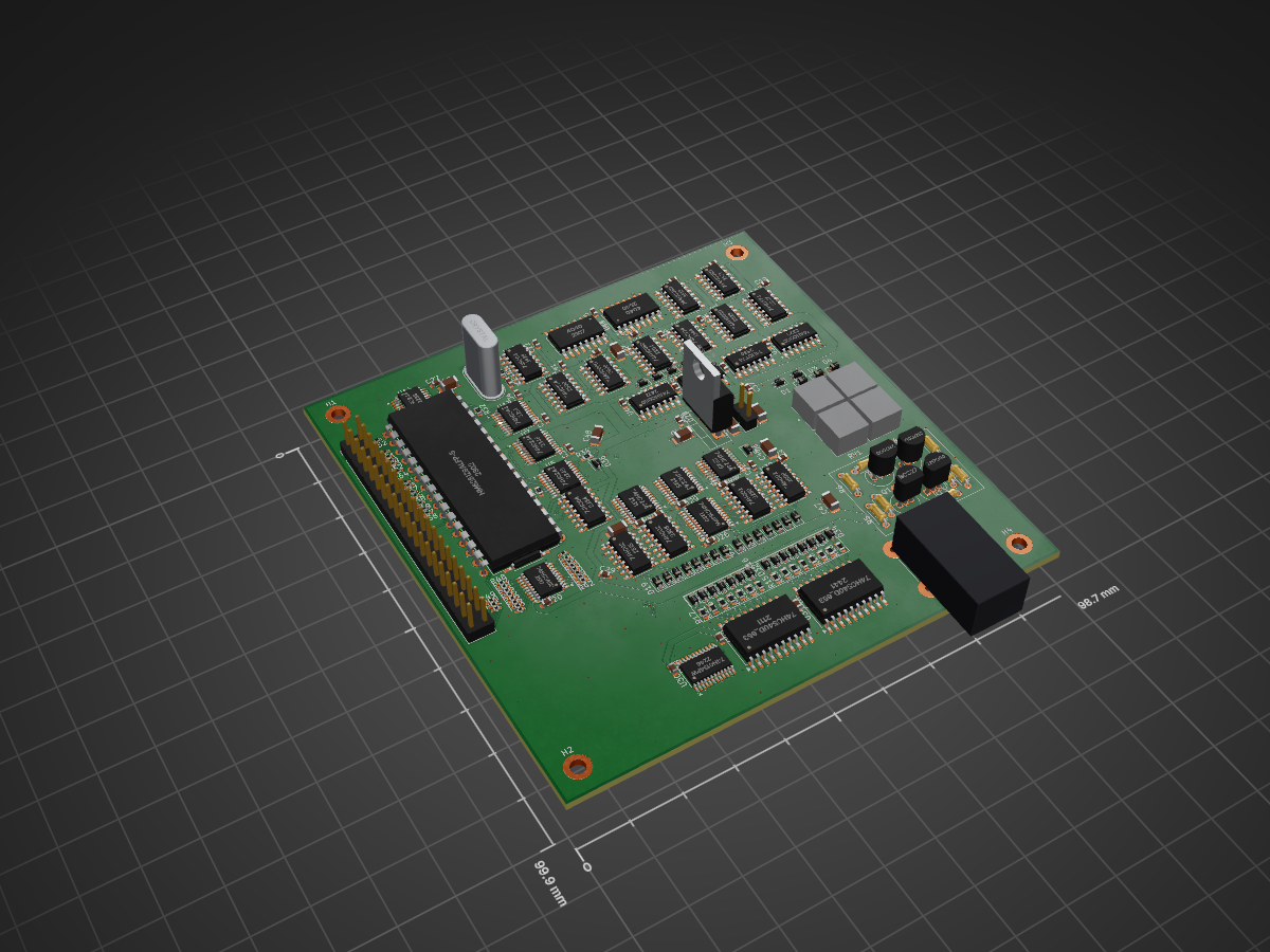
ntsc sync with 74xx logic gates
Ntscv2 is an open-source printed circuit board by xp5-org, from the xp5-org/ntsc-framebuffer repository on GitHub, published under the MIT licence. It is a 4-layer board of 98.7 × 99.9 mm with 225 parts on 352 nets, routed with 5,150 tracks and 624 vias.
It is built around the 74HC244D, 74HC245D and 74AHC08D, with the 74HCT74D, 74HC02 and 74HC04D among its other parts. Its parts include 68 resistors, 49 capacitors, 41 diodes, 38 ICs and 4 transistors.


NTSC framebuffer built around 74x cmos logic gates and an 128k x 8bit sram module
** this is incomplete and not yet built, in-progress **
Tasks remaining:
This is the core of the circuit, its two 4040 counters, one driving the other. the first counts out 454 which is the number of inactive + active horizontal pixels per row. the output is binary, and with enough AND gates alongside numerous D type flipflops, specific events can be timed out and set to form the sync timings needed
vertical reset is checked at the end of the horizontal scanline, so we use _HRESET as the clock for vreset - the condition of 261V lines is set only when _HRESET is ready
the circuit starts off with some DC bias to give a sync tip from the "previous" scanline, and then at H2 + H8 HBLANK-ENABLE flop is cycled on. When this is on, elsewhere in the circuit the bias is cut off and gives us the horizontal sync tip
When H2 + H8 + H32 is seen (H42) , HBLANK_DISABLE is turned on, which is a 2nd flop "HSYNC B"
this lets me chain the hsync events together with explicit start and stop events, block them from re-triggering
the 4-16 mux is often used for memory addressing and is only available in active-low, so in this case im using NOR gates to invert the signal . the MUX outputs are always high-inactive, so all NOR gates except for the active one are getting a positive voltage which turns them all off, exxcept for the active-low received from the MUX, this NOR gate switches on and provides a color clock at specific delays introduced by the 74AHC451's 4-5ns gate propigation delay
The output-amplifier interfaces the low-current, low impedience CMOS or TTL logic with the 1.4v, 75-ohm composite.
HSYNC, Colorburst, and Pixel Input are given to the amplifiers input. Its first passed through a 2n7000 N-channel mosfet which inverts the signal. This drives a PNP transistor to return it back to positive output, this allowed the GND of the composite-out to also be the same reference plane as the GND of this circuit (pnp could be omitted and use only mosfet with resistor network and floating Gnd)
This has two additional mosfets for saturation bias and output voltage reduction (brightness). The saturation mosfet biases the PNPs turnoff point "upwards" so that its off point rises above what hsync/hblank would have been . this serves the purpose of adding DC bias to reduce the modulation of the output without affecting the output peak (overall brightness). in summary, this is an amplifier which can control the height of the bottoms and tops of the wave output separately. its needed for color, but could dispose of half the mosfets if it were used for monochrome
LTSpice Model of Output Amplifier
output amplifier in ltspice, showing peak brightness vs minimum brightness pixels , there is some distortion in the sim. Some gates are switching on/off before others and causing brief voltage spikes, this might be ignorable on the physical circuit ill have to go through the circuit flow to see what the issue is
| Qty | Value | Footprint | References |
|---|---|---|---|
| 37 | C | Capacitor_SMD:C_0603_1608Metric | C10, C11, C12, C13, C14, C15, C17, C19, C20, C21, C22, C23, C24, C25, C26, C27 +21 |
| 36 | 10k | Resistor_SMD:R_0402_1005Metric_Pad0.72x0.64mm_HandSolder | R30, R33, R35, R36, R37, R38, R39, R40, R41, R42, R43, R44, R45, R46, R47, R48 +20 |
| 31 | 1N4148 | Diode_SMD:D_SOD-323 | D10, D11, D12, D13, D14, D15, D16, D17, D18, D19, D20, D21, D22, D23, D24, D25 +15 |
| 17 | R | Resistor_SMD:R_0603_1608Metric | R10, R15, R16, R17, R18, R19, R20, R21, R22, R23, R24, R25, R26, R27, R28, R29 +1 |
| 10 | 1N4448 | Diode_SMD:D_SOD-323 | D1, D2, D3, D4, D5, D36, D37, D38, D41, D42 |
| 10 | R | Resistor_THT:R_Axial_DIN0204_L3.6mm_D1.6mm_P5.08mm_Horizontal | R2, R3, R4, R5, R6, R7, R11, R12, R13, R14 |
| 8 | 20uF 16v | Capacitor_SMD:C_1206_3216Metric | C42, C43, C44, C45, C46, C47, C48, C49 |
| 8 | 74HC244 | Package_SO:TSSOP-20_4.4x6.5mm_P0.65mm | U5, U6, U7, U12, U13, U27, U29, U31 |
| 7 | 74AHC08D | Package_SO:SO-14_3.9x8.65mm_P1.27mm | U1, U2, U3, U4, U15, U16, U38 |
| 5 | 74HCT74 | Package_SO:SO-14_3.9x8.65mm_P1.27mm | U8, U9, U10, U11, U19 |
| 4 | 4040 | Package_SO:SOIC-16W_5.3x10.2mm_P1.27mm | U18, U21, U23, U24 |
| 4 | 74HC02 | Package_SO:SOIC-14_3.9x8.7mm_P1.27mm | U32, U33, U36, U37 |
| 4 | MountingHole_Pad | MountingHole:MountingHole_2.7mm_M2.5_DIN965_Pad | H1, H2, H3, H4 |
| 3 | 10k | Resistor_SMD:R_0603_1608Metric | R31, R32, R34 |
| 3 | 2N7000 | Package_TO_SOT_THT:TO-92_Inline | Q1, Q2, Q4 |
| 3 | R_Potentiometer | mysymbols_footprint:TRIM_3362P-1-100LF | RV1, RV2, RV4 |
| 2 | 10uF 25V | Capacitor_SMD:C_1206_3216Metric | C50, C51 |
| 2 | 15pF | Capacitor_SMD:C_0603_1608Metric | C1, C2 |
| 2 | 74HC04 | Package_SO:SOIC-14_3.9x8.7mm_P1.27mm | U22, U25 |
| 2 | 74HC154PW | Package_SO:TSSOP-24_4.4x7.8mm_P0.65mm | U26, U30 |
| 2 | 74HC540D_653 | Package_SO:SOIC-20W_7.5x12.8mm_P1.27mm | U34, U35 |
| 1 | 100R | mysymbols_footprint:TRIM_3362P-1-100LF | RV3 |
| 1 | 6k | Resistor_SMD:R_0603_1608Metric | R1 |
| 1 | 74HC244 | Package_SO:SSOP-20_4.4x6.5mm_P0.65mm | U14 |
| 1 | 74HC245D | Package_SO:TSSOP-20_4.4x6.5mm_P0.65mm | U20 |
| 1 | BC327 | Package_TO_SOT_THT:TO-92_Inline | Q3 |
| 1 | CBEN | mysymbols_footprint:TestPoint_Pad_0.8x0.8mm | TP85 |
| 1 | CB_DIS | mysymbols_footprint:TestPoint_Pad_0.8x0.8mm | TP86 |
| 1 | CB_Source | mysymbols_footprint:TestPoint_Pad_0.8x0.8mm | TP5 |
| 1 | Conn_01x02 | Connector_PinHeader_2.54mm:PinHeader_1x02_P2.54mm_Vertical | J3 |
| 1 | Conn_02x20_Odd_Even | Connector_PinHeader_2.54mm:PinHeader_2x20_P2.54mm_Vertical | J1 |
| 1 | Conn_Coaxial | Connector_Coaxial:BNC_TEConnectivity_1478035_Horizontal | J2 |
| 1 | Crystal | Crystal:Crystal_HC49-U_Vertical | Y1 |
| 1 | FIELD0 | mysymbols_footprint:TestPoint_Pad_0.8x0.8mm | TP88 |
| 1 | FIELD1 | mysymbols_footprint:TestPoint_Pad_0.8x0.8mm | TP87 |
| 1 | HM628128ALFP-5 | Package_DIP:DIP-32_W15.24mm | U17 |
| 1 | HRESET | mysymbols_footprint:TestPoint_Pad_0.8x0.8mm | TP82 |
| 1 | HSYNCA | mysymbols_footprint:TestPoint_Pad_0.8x0.8mm | TP80 |
| 1 | HSYNCB | mysymbols_footprint:TestPoint_Pad_0.8x0.8mm | TP79 |
| 1 | HSYNC_input | mysymbols_footprint:TestPoint_Pad_0.8x0.8mm | TP7 |
| 1 | LM7805_TO220 | Package_TO_SOT_THT:TO-220-3_Vertical | U28 |
| 1 | PIXELDRAWEN | mysymbols_footprint:TestPoint_Pad_0.8x0.8mm | TP84 |
| 1 | Pixeldrive_input | mysymbols_footprint:TestPoint_Pad_0.8x0.8mm | TP6 |
| 1 | VBLANK | mysymbols_footprint:TestPoint_Pad_0.8x0.8mm | TP81 |
| 1 | VRESET | mysymbols_footprint:TestPoint_Pad_0.8x0.8mm | TP83 |
| 1 | ~ | Resistor_SMD:R_0603_1608Metric | R8 |


It measures 98.7 × 99.9 mm and has 4 copper layers, 1.6 mm thick.
225 parts, built around the 74HC244D, 74HC245D, 74AHC08D and 74HCT74D. The full list of its parts is on this page, with links to each part's symbol and footprint where PCBKit's library has them.
From the xp5-org/ntsc-framebuffer repository on GitHub, at the commit this page was made from: the board is ntscv2/ntscv2.kicad_pcb and its schematic ntscv2/ntscv2.kicad_sch. PCBKit opens the board in the browser, with nothing to install.
Its repository publishes it under the MIT licence: you may reuse it on that licence's terms (keep the author's notice, and for a copyleft licence share your changes alike).