2 layers94.9 × 105.2 mm
Stencil
wselsbe/optacon
This project aims to recreate the Optacon (OPtical to TActile CONverter), a reading aid for the blind. The user moves a small camera module over a document to scan one letter at a time.
122 parts

 wselsbe/optacon
This project aims to recreate the Optacon (OPtical to TActile CONverter), a reading aid for the blind. The user moves a small camera module over a document to scan one letter at a time.
Connector is an open-source printed circuit board by wselsbe, from the wselsbe/optacon repository on GitHub. It is a 2-layer board of 22.7 × 33.2 mm with 3 parts on 14 nets, routed with 64 tracks and 0 vias.
This project aims to recreate the Optacon (OPtical to TActile CONverter), a reading aid for the blind. The user moves a small camera module over a document to scan one letter at a time. The main module has a "tactile display": a 6x24 array of vibrating pins, so the user can feel the shape of the letter being scanned with their fingertip.
The vibrating pins are actuated by piezoelectric bimorphs, similar to those used in refreshable braille displays. The Optacon uses vibrating pins instead of static, and achieves a higher pin density: 1mm x 2mm versus 2.5mm x 2.5mm. The following videos show the display in action. The piezo bimorphs actuate at around 250Hz, the motion appears slowed down by a stroboscopic led.
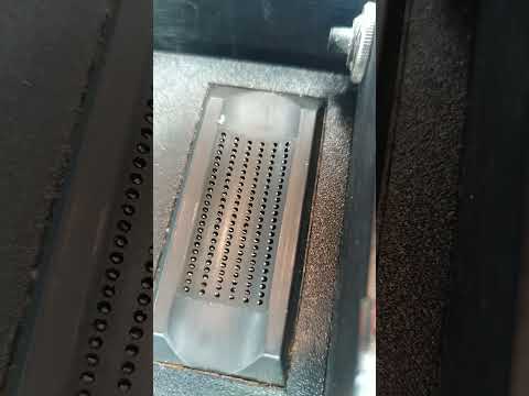
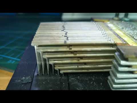
The high density tactile display remains state of the art. Even now, 50 years later, there is no technology available that achieves the same high density while still remaining portable and battery powered.
The smallest commercially available piezoelectric actuators are those meant for braille cells, and are 2.5mm wide. No piezo manufacturer wanted to try to create narrower actuators.
My solution is to start with an off the shelf 40mm x 20mm x 0.9mm actuator, and dice it into 20 individual parallel actuators with a wafer dicing saw. This uses a very precise air bearing spindle with a very thin (55 micron) diamond blade to cut through the piezoceramic. Because the blade is water cooled, the piezoceramic actuator remains below the curie temperature (about 150°C) and does not lose its polarisation.
Holding the actuators during and after dicing proved challenging. Typically silicon wafers are mounted with UV dicing tape, but this tape is expensive. Another potential solution is heat release tape, where the adhesive softens at higher temperature (but still below the piezoceramic curie temperature), but this is similarly expensive.
I got some success by using Crystalbond 509: by heating it to 74°C on a hotplate I could apply the adhesive to a glass disc, add the piezoceramic, and letting the adhesive cool down to harden. The disc is then held in place the the dicing saw's vacuum chuck. But transferring the diced actuators to a pcb, while still remaining parallel after dicing, proved to be too difficult. The Crystalbond 509 has to be released by using heat and a solvent (acetone), without affecting the second adhesive used to attach the piezoceramic reeds to the pcb.
The key proved to be in reversing the steps.
The actuator board is designed around 2 components: a high voltage piezo driver, and high voltage shift registers . All components are chosen for small size and low height, to keep the boards stackable. The tallest component is the inductor at 1.2mm. The passive components are 0603 for manual pick and place.
The TI DRV2665 can output 100V with only an inductor and capacitor. It has an I2C interface and an analog input. Alternatives are DRV2667 (pin compatible) and DRV8667 & DRV2700 (analog only) The inductor TDK VLS3012HBX-3R3M is chosen for low height, low resistance (150mΩ), and high current (2.37A temp rating). The capacitor is rated for 200V. TI has an excel sheet to help calculate the values for the inductor, capacitor, and feedback resistors.
To increase the efficiency the piezo driver is powered from VIN (battery or usb). The I2C lines are pulled up to VDD (3.3V), compatible down to 1.8V
The piezo driver has a differential output, which can drive piezos at 200V peak to peak. Because of the shift registers only one output (up to 100V) is used. Without input the outputs float at half the boost voltage, ideally the external controller should make sure the input is pulled down.
The I2C and analog input pins are broken out to the FFC connector.
The Microchip HV509 high voltage shift registers are used to address the individual piezo actuators. There are no real alternatives available in QFN or similar low height package. The common BP pin is connected to the common bottom & top electrodes on the piezos. The individual outputs go to the center electrodes. There are 16 outputs per shift registers, 10 are used on each shift register, the other 6 are unused. Diode D1 is needed to bias the output transistors to at least VDD before the high voltage is enabled. The datasheet says the minimum voltage is 50V for the outputs to switch. In practice this does not look like a major issue: if the HV is a sine wave they might switch late, but will still pass through the lower voltage after switching. (Needs further testing)
Both shift registers are chained together, the SPI pins (clock, data in, data out) and Latch and Polarity are broken out to the FFC connector
The motherboard is designed to drive several actuator boards (up to 6), a future revision will accept external input such as a camera to read printed letters. It's based on an ESP32-S3-WROOM-1 module. Currently the goal of the motherboard is to act as a controller and interface to the actuator boards. At first, the firmware should simply generate a sinewave and step through the individual actuators, as a test for the actuator boards.
| Qty | Value | Footprint | References |
|---|---|---|---|
| 2 | Conn_01x12_MountingPin | Optacon_common:Hirose_FH34SRJ-12S-0.5SH | J1, J2 |
| 1 | Conn_01x12 | Connector_PinHeader_2.54mm:PinHeader_1x12_P2.54mm_Vertical | J3 |
It measures 22.7 × 33.2 mm and has 2 copper layers, 1.6 mm thick.
3 parts. The full list of its parts is on this page, with links to each part's symbol and footprint where PCBKit's library has them.
From the wselsbe/optacon repository on GitHub, at the commit this page was made from: the board is connector/connector.kicad_pcb and its schematic actuator/actuator.kicad_sch. PCBKit opens the board in the browser, with nothing to install.
Its repository states no licence, so its author keeps all rights: ask wselsbe before reusing the design.
wselsbe/optacon
This project aims to recreate the Optacon (OPtical to TActile CONverter), a reading aid for the blind. The user moves a small camera module over a document to scan one letter at a time.

wselsbe/optacon
This project aims to recreate the Optacon (OPtical to TActile CONverter), a reading aid for the blind. The user moves a small camera module over a document to scan one letter at a time.

wselsbe/optacon
This project aims to recreate the Optacon (OPtical to TActile CONverter), a reading aid for the blind. The user moves a small camera module over a document to scan one letter at a time.

wselsbe/optacon
This project aims to recreate the Optacon (OPtical to TActile CONverter), a reading aid for the blind. The user moves a small camera module over a document to scan one letter at a time.


hzeller/rpi-rgb-led-matrix
Controlling up to three chains of 64x64, 32x32, 16x32 or similar RGB LED displays using Raspberry Pi GPIO


atopile/atopile
Design circuit boards with code! ✨ Get software-like design reuse 🚀, validation, version control and collaboration in hardware; starting with electronics ⚡️


hackclub/sprig
🍃 Learn to code by making games in a JavaScript web-based game editor.