
4 layers18.9 × 27.5 mm
Modchip poe
wrcrooks/rtlplayground-modchip
RP2350 management board for RTL8372 switches (SWTG024AS-V2.0): KiCad hardware, MicroPython tools and design notes; pairs with the bridge firmware in wrcrooks/RTLPlayground
44 partsMIT

RP2350 management board for RTL8372 switches (SWTG024AS-V2.0): KiCad hardware, MicroPython tools and design notes; pairs with the bridge firmware in wrcrooks/RTLPlayground
Modchip is an open-source printed circuit board by wrcrooks, from the wrcrooks/rtlplayground-modchip repository on GitHub, published under the MIT licence. It is a 4-layer board of 56.9 × 37.2 mm with 53 parts on 66 nets, routed with 432 tracks and 82 vias.
It is built around the RP2350A, W25Q128JVSIQ and LM66100DCK. Its parts include 21 capacitors, 20 resistors, 4 connectors, 3 ICs and 1 diode. It belongs with the RP2350 boards of this library.


A second board for the PoE switch (PCB 2M-PCB49-V1.1, RTL8372 with 2 MiB of flash): the same RP2350
circuit as the SWTG024AS-V2.0 board in ../, cut down to what this switch offers and made as small as
it can be.
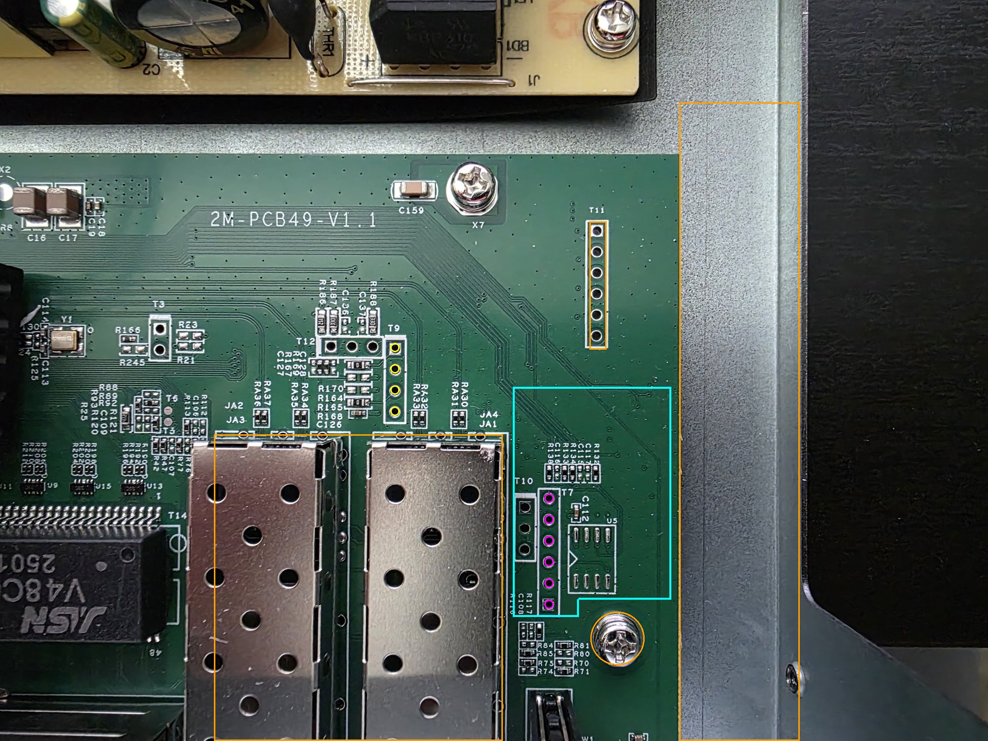
Status: designed and routed with a clean DRC. Not built yet. The T7 and T9 signal pins are guesses. Check them before ordering (see the end of this page).
| File | What |
|---|---|
modchip-poe.kicad_pcb, modchip-poe.kicad_pro | KiCad 10 board. The outline is on Edge.Cuts and J1 is on the bottom side on T7's holes. The switch's parts are drawn on Dwgs.User and notes are on Cmts.User. The aux and grid origin is T7 pin 1 |
make_pcb.py, build.sh, modchip-poe.kicad_dru | Layout and routing pipeline (as in ../, with ../finish.py), and JLCPCB's design rules |
modchip-poe.kicad_sch, schematic-poe.pdf | Schematic, and a PDF of it |
make_sch.py | Generates the schematic. It uses ../make_sch.py's generator and lists every pin's net |
check_sch.py, expected-nets.json | ERC, plus KiCad's netlist compared pin by pin with the intended nets |
outline.py, overlay.jpg | The outline, T7/T9/T10 and the obstacles in one place. Running it checks the clearances; --photo draws them on the photo |
lib/ | Footprints for U5 and L1, imported from LCSC, and L1's 3D model. U5 uses KiCad's Winbond USON-8 model |
production/ | JLCPCB files: Gerbers and drill zip, BOM, positions |
mechanical/ | STL and STEP of the assembled board, without J1/J3/J5, for a printed fit check |
Rebuild everything from the schematic to the production files with:
KAK=~/Desktop/Workspace/KiCad/kicad-agent-kit ./build.sh
python3 outline.py --photo headers.jpg # RTLPlayground doc/devices/photos/2M-PCB49-V1.1/headers.jpgThe circuit is that of ../make_sch.py, with these changes:
No USB. Power comes from the switch's 3.3 V on T7 pin 4, through the LM66100 ideal diode U2. Programming and debug go over SWD (J5).
Bench power. A debug probe can power the board on J5 pin 1; U2 keeps that supply out of the switch.
Flash. U5 is a W25Q16JVUXIQ, 2 MiB in USON-8 2×3 mm, fitted with an RP2350A. The RP2354A has the same 2 MiB inside its package, but JLC has only a handful in stock. With an RP2354A in U1's place, leave U5 and C19 off.
Not on this board. There is no T8-style GPIO header, since this switch has none, and no reset driver, since no reset point is known.
GPIO use is the same as the first board, so the firmware's pin map holds:
| GPIO | Use |
|---|---|
| GP0 / GP1 | UART0 |
| GP11 / GP10 | I²C1 SCL / SDA |
| GP9 / GP8 | T7 pins 5 / 6 |
| GP22 | LED |
| GP26 | Switch-power sense |
Series resistors and pull-ups. Every line to the switch has 100 Ω in series. The I²C lines have 4.7 kΩ pull-ups to the switch's 3.3 V.
| Pad | Signal |
|---|---|
| J1 (into T7) | 1 SCL, 2 GND, 3 SDA, 4 3.3 V from the switch, 5 GP9, 6 GP8 |
| J3 (wires to T9, pad n to pin n) | 1 the switch's U0TXD, 2 GND, 3 the switch's U0RXD, 4 not connected |
| J5 (SWD, 1.27 mm) | 1 3.3 V, 2 SWCLK, 3 GND, 4 SWDIO, 5 RUN |
python3 check_sch.py reports a clean ERC and all 168 pins on their intended nets (33 nets).
The board has 4 layers, 1.0 mm thick:
| Layer | Use |
|---|---|
| F.Cu | Parts, signals and a GND pour |
| In1 | GND |
| In2 | +3V3 |
| B.Cu | Signals and a GND pour |
Only J1 is on the bottom side. make_pcb.py places these parts by hand:
The other parts are auto-placed. Locked hand routes cover:
Freerouting routes the rest, with analytics and telemetry off on its command line. The result has no DRC errors or warnings and is fully connected.
production/)Board. 4 layers, 1.0 mm thick, 0.2 mm minimum via drill.
Assembly. PCBA on the top side only: 41 parts, 18 BOM lines, every line with an LCSC number.
Parts. All are in stock as of 2026-11-02. Basic parts throughout, except five Extended ones:
| Part | LCSC | Stock |
|---|---|---|
| RP2350A | C42411118 | 4,697 |
| W25Q16JVUXIQ | C2843335 | 450 |
| ABM8 crystal | C20625731 | 8,774 |
| LM66100 | C2869734 | 11,326 |
| 3.3 µH inductor, FNR201610S3R3MT | C167673 | 1,380 |
The inductor. The first board's AOTA-B201610S3R3 (C42411119, the part the RP2350 datasheet names) is down to 1 in stock. This board uses a shielded 2016 3.3 µH instead, rated 880 mA, plenty for the core supply. The first board's BOM needs the same substitute until the AOTA is back.
Not assembled. J1 is a 1×6 2.54 mm male header, hand-soldered from below. J3 and J5 are bare pads.
Check in JLC's preview. The rotation of U1, U5 (USON-8), U2, Y1 and L1.
mechanical/modchip-poe-no-headers.stl or lay a 1:1 print of the outline on the switch.-DMODCHIP_BOARD=poe (firmware/rp2350/README.md) and the
8051 bridge with MACHINE=POE_2G040210GSM, plus the PoE image (RTLPlayground's
modchip/bridge/README.md). Neither has run on this switch yet.| Qty | Value | Footprint | References |
|---|---|---|---|
| 13 | 100n | Capacitor_SMD:C_0402_1005Metric | C1, C2, C3, C4, C5, C6, C7, C8, C9, C10, C11, C12, C19 |
| 10 | 100 | Resistor_SMD:R_0402_1005Metric | R10, R11, R12, R13, R14, R15, R16, R17, R18, R19 |
| 4 | 4.7u | Capacitor_SMD:C_0402_1005Metric | C13, C14, C15, C16 |
| 3 | 100k | Resistor_SMD:R_0402_1005Metric | R22, R23, R24 |
| 2 | 15p | Capacitor_SMD:C_0402_1005Metric | C17, C18 |
| 2 | 1k | Resistor_SMD:R_0402_1005Metric | R6, R25 |
| 2 | 4.7k | Resistor_SMD:R_0402_1005Metric | R20, R21 |
| 1 | 10k | Resistor_SMD:R_0402_1005Metric | R8 |
| 1 | 10u | Capacitor_SMD:C_0603_1608Metric | C22 |
| 1 | 12MHz | Crystal:Crystal_SMD_3225-4Pin_3.2x2.5mm | Y1 |
| 1 | 1u | Capacitor_SMD:C_0402_1005Metric | C24 |
| 1 | 2N7002 | Package_TO_SOT_SMD:SOT-23 | Q1 |
| 1 | 3.3uH | Inductor_SMD:L_Murata_DFE201610P | L1 |
| 1 | 33 | Resistor_SMD:R_0402_1005Metric | R5 |
| 1 | 330 | Resistor_SMD:R_0402_1005Metric | R9 |
| 1 | LM66100 | Package_TO_SOT_SMD:SOT-363_SC-70-6 | U2 |
| 1 | RP2350A | Package_DFN_QFN:QFN-60-1EP_7x7mm_P0.4mm_EP3.4x3.4mm_ThermalVias | U1 |
| 1 | Reset wire to D3 anode | TestPoint:TestPoint_THTPad_D1.5mm_Drill0.7mm | TP1 |
| 1 | SWD | Connector_PinHeader_1.27mm:PinHeader_1x05_P1.27mm_Vertical | J5 |
| 1 | To switch T3 (I2C slave) | Connector_PinHeader_2.00mm:PinHeader_1x06_P2.00mm_Vertical | J1 |
| 1 | To switch T5 (UART0) | Connector_PinHeader_2.54mm:PinHeader_1x04_P2.54mm_Vertical | J3 |
| 1 | To switch T8 (GPIO46-49) | Connector_PinHeader_2.00mm:PinHeader_1x06_P2.00mm_Vertical | J2 |
| 1 | W25Q128JVSIQ | Package_SO:SOIC-8_5.3x5.3mm_P1.27mm | U5 |
| 1 | red | LED_SMD:LED_0603_1608Metric | D1 |
It measures 56.9 × 37.2 mm and has 4 copper layers, 1 mm thick.
53 parts, built around the RP2350A, W25Q128JVSIQ and LM66100DCK. The full list of its parts is on this page, with links to each part's symbol and footprint where PCBKit's library has them.
From the wrcrooks/rtlplayground-modchip repository on GitHub, at the commit this page was made from: the board is hardware/modchip.kicad_pcb and its schematic hardware/modchip.kicad_sch. PCBKit opens the board in the browser, with nothing to install.
Its repository publishes it under the MIT licence: you may reuse it on that licence's terms (keep the author's notice, and for a copyleft licence share your changes alike).
wrcrooks/rtlplayground-modchip
RP2350 management board for RTL8372 switches (SWTG024AS-V2.0): KiCad hardware, MicroPython tools and design notes; pairs with the bridge firmware in wrcrooks/RTLPlayground

xXsenseiXx/KHATAF-F411
Open-hardware 4-layer STM32F411 drone flight controller designed in KiCad for INAV and Betaflight.

Arhamee/hardware-portfolio
Multi-layer PCB designs in KiCad 10 schematic capture to fabrication-ready Gerbers. High-speed routing, BGA escape, power electronics.

coco-chameleon/chameleon-hardware
TRS-80 Color Computer cartridge emulator

gorkemguven/RP2040-Dual-TypeC-eMMC-Board
A 4-layer embedded development board featuring RP2040, USB2244 high-speed eMMC bridge, dual Type-C ports, and INA226/TMP119 power & telemetry monitoring.

pinanshu123/High-Speed-USB-2.0-Storage-Device-PCB

SshgurkiratSingh/CCMS_PORTAL
A full-stack smart streetlight fleet management system with real-time monitoring, remote control, and analytics.


profdc9/PicoAlt2
An alternative Pi Pico 2 (RP2350) type board you can have made yourself.