
2 layers105.4 × 215.6 mm
MIDI Sax
hackclub/OnBoard
💡 Join 1,000 teenagers and make your first PCB with a $100 grant!
75 parts915

 whatnick/ADE9000_Breakout
ADE9000 Energy Monitor Breakout from Analog Devices
ADE9000 Breakout is an open-source printed circuit board by whatnick, from the whatnick/ADE9000_Breakout repository on GitHub. It is a 2-layer board of 65 × 55 mm with 75 parts on 55 nets, routed with 521 tracks and 38 vias.
Its parts include 32 resistors, 25 capacitors, 4 connectors, 1 IC and 1 diode. It belongs with the interfaces and adapters boards of this library.
Breadboard-compatible breakout for the Analog Devices ADE9000 — a high-performance, multiphase energy and power quality monitoring IC.
The board follows the test circuit from Figure 55 of the ADE9000 datasheet (Rev. B, p. 28): all onboard passives (decoupling, RC anti-aliasing filters, crystal load caps, reset RC) are populated, power plus the analog channels are broken out to 0.1" headers, and the remaining digital signals are exposed on test pads to keep the board compact.
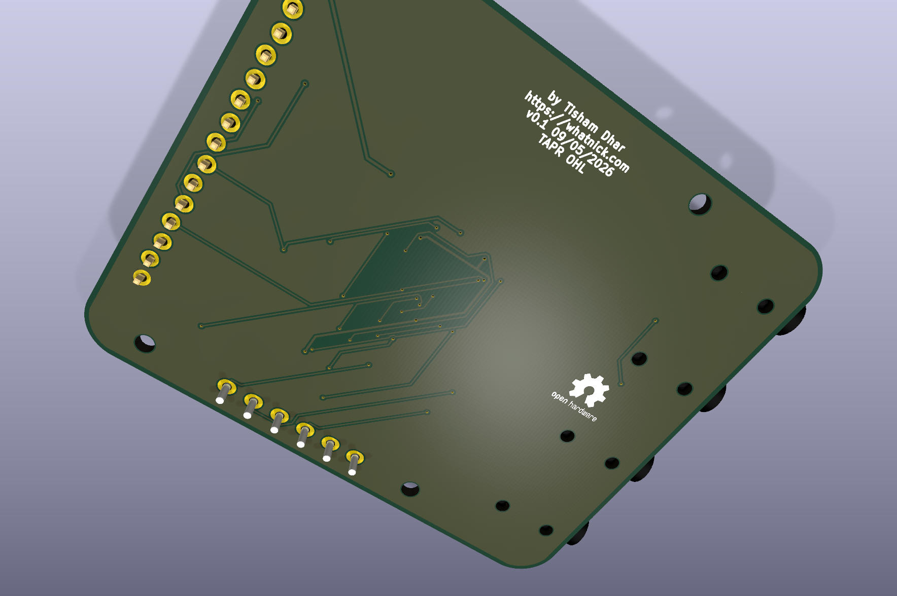
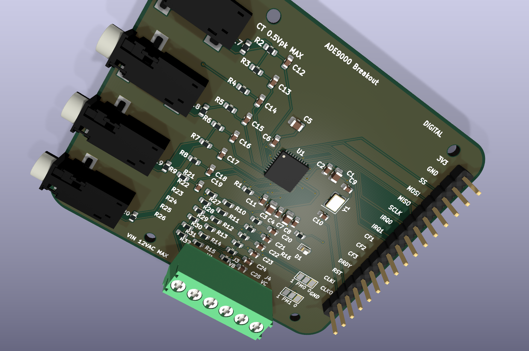
These views are rendered from the populated KiCad assembly using the project-local STEP models.
| Top isometric | Bottom isometric |
|---|---|
 |  |
| Pin | Signal | ADE9000 Pin | Description |
|---|---|---|---|
| 1 | 3.3V | — | Power in |
| 2 | GND | — | Ground |
| Pin | Signal | ADE9000 Pin | Description |
|---|---|---|---|
| 1 | IAP | 7 | Phase A current, positive |
| 2 | IAN | 8 | Phase A current, negative |
| 3 | IBP | 9 | Phase B current, positive |
| 4 | IBN | 10 | Phase B current, negative |
| 5 | ICP | 11 | Phase C current, positive |
| 6 | ICN | 12 | Phase C current, negative |
| 7 | INP | 13 | Neutral current, positive |
| 8 | INN | 14 | Neutral current, negative |
Each input pair has a 1 kΩ series resistor and 22 nF cap to GND already fitted on board. Max differential input ±1 V / PGA gain.
| Pin | Signal | ADE9000 Pin | Description |
|---|---|---|---|
| 1 | VAP | 20 | Phase A voltage, positive |
| 2 | VAN | 19 | Phase A voltage, negative |
| 3 | VBP | 22 | Phase B voltage, positive |
| 4 | VBN | 21 | Phase B voltage, negative |
| 5 | VCP | 24 | Phase C voltage, positive |
| 6 | VCN | 23 | Phase C voltage, negative |
Each input pair has the same 1 kΩ + 22 nF RC filter as the current inputs.
| Pad | Signal | ADE9000 Pin | Description |
|---|---|---|---|
| TP1 | SS | 40 | SPI slave select (active low) |
| TP2 | MOSI | 39 | SPI data in |
| TP3 | MISO | 38 | SPI data out |
| TP4 | SCLK | 37 | SPI clock (up to 20 MHz) |
| TP5 | IRQ0 | 31 | Interrupt output 0 (active low) |
| TP6 | IRQ1 | 32 | Interrupt output 1 (active low) |
| TP7 | CF1 | 33 | Calibration frequency output 1 |
| TP8 | CF2 | 34 | Calibration frequency output 2 / LED drive |
| TP9 | CF3_ZX | 35 | Zero-cross / CF3 output |
| TP10 | CF4_DREADY | 36 | Data-ready / event / CF4 output |
| TP11 | RESET | 6 | Reset (active low, RC-held high) |
JP1 controls PM0 and JP2 controls PM1. Each open three-pad jumper is marked
1 PMx 0: bridge the center pad to 1 for +3V3, or to 0 for GND.
| JP2 / PM1 | JP1 / PM0 | Selection |
|---|---|---|
| 0 | 0 | Normal operation |
| 0 | 1 | PM1:PM0 = 01 |
| 1 | 0 | PM1:PM0 = 10 |
| 1 | 1 | PM1:PM0 = 11 |
Bridge exactly one side of each jumper before powering the board. Never bridge
both sides, and do not leave a mode pin floating. Production boards intended
for normal operation should have the 0 side bridged on both JP1 and JP2.
A 24.576 MHz crystal is fitted between CLKIN (pin 29) and CLKOUT (pin 30) with 16 pF load capacitors to GND. This matches the ADE9000's required ±30 ppm clock.
To use an external clock instead, remove the crystal, leave the load caps unpopulated, and drive CLKIN directly (3.3 V logic, 24.330–24.822 MHz, 45:55–55:45 duty cycle).
The ADE9000 uses SPI mode 0 (CPOL=0, CPHA=0), MSB first, up to 20 MHz.
| Signal | Direction (from MCU) | Notes |
|---|---|---|
| SCLK | Output | Max 20 MHz |
| MOSI | Output | 16-bit or 32-bit transfers |
| MISO | Input | |
| SS | Output | Assert low before each transfer |
All SPI pins are 3.3 V logic. Use a level shifter if connecting to a 5 V MCU.
The onboard RC filter on each analog input pin:
Signal ──[ 1 kΩ ]──┬── IxP / VxP (ADE9000 pin)
                   │
                 [22 nF]
                   │
                  GND
This provides a first-order anti-aliasing LPF with fc ≈ 7.2 kHz, matching the ADC's −3 dB bandwidth. For CT or Rogowski coil inputs, drive the differential pair through an additional burden resistor or signal conditioning stage before these onboard filters.
Source purchasing fields live on the schematic symbols as Manufacturer, MPN, DigiKey, Mouser, and Description properties. Regenerate the grouped purchasing BOM with:
& "C:\Program Files\KiCad\10.0\bin\python.exe" .\scripts\apply_bom_fields.py
& "C:\Program Files\KiCad\10.0\bin\python.exe" .\scripts\export_bom.py --html .\bom\ADE9000_Breakout_BOM.html
Generated outputs are available as bom/ADE9000_Breakout_BOM.csv, bom/ADE9000_Breakout_BOM.xlsx, and bom/ADE9000_Breakout_BOM.html. The DigiKey and Mouser fields use distributor search URLs for the selected manufacturer MPNs so stock and packaging can be checked at order time.
| Ref | Value | Package | Notes |
|---|---|---|---|
| U1 | ADE9000 | CP-40-7 LFCSP | Main IC |
| Y1 | 24.576 MHz | 3225 (3.2×2.5 mm) | ±30 ppm |
| C_CLKIN, C_CLKOUT | 16 pF | 0402 | Crystal load caps |
| C_VDD1 | 10 µF | 0805 | VDD bulk decoupling |
| C_VDD2, C_AVDD2, C_DVDD2, C_REF2 | 0.1 µF | 0402 | HF decoupling |
| C_AVDD1, C_DVDD1, C_REF1 | 4.7 µF | 0805 | LF decoupling |
| C_RST | 1 µF | 0402 | Reset RC |
| C_PM | 1 µF | 0402 | PM0 bypass |
| R_RST | 10 kΩ | 0402 | Reset pull-up |
| R_IAP…R_VCN (×14) | 1 kΩ | 0402 | Anti-aliasing series R |
| C_IAP…C_VCN (×7) | 22 nF | 0402 | Anti-aliasing cap (differential) |
| R_LED | 1 kΩ | 0402 | CF2 LED current limit |
| D_LED | Green LED | 0402 | CF2 activity indicator |
The KiCad schematic (ADE9000_Breakout.kicad_sch) implements Figure 55 of the datasheet with compact breakout constraints: only power and analog channels go to headers, while digital signals stay on test pads. Reference images and the datasheet are in docs/.
Project-local STEP models for all populated ADE9000 board parts are stored in models/step/. The PCB references these files through ${KIPRJMOD} so the 3D view and CAD export do not depend on a particular KiCad library installation.
The digital/debug header J1 uses SparkFun's staggered 1x16_Locking friction-fit footprint, vendored at footprints/SparkFun-Connector.pretty/1x16_Locking.kicad_mod from sparkfun/SparkFun-KiCad-Libraries commit 14865e2. It keeps the 2.54 mm header pitch but alternates pad positions by 0.127 mm so a standard breakaway male header can lock into the board without solder during bench use. The SparkFun library is licensed CC BY 4.0; attribution: SparkFun Electronics.
The stereo CT jacks use a black AP214-colored STEP model at models/step/Jack_3.5mm_CUI_SJ-3523-SMT_Horizontal.step, generated from the manufacturer SJ-3523-SMT-TR CAD ZIP in models/step/SJ_3523_SMT_TR.zip with scripts/create_sj3523_smt_step.py. The script bakes the DigiKey/Same Sky CAD into the KiCad footprint frame with the front barrel on the footprint's board-edge side, without adding artificial pad overlays. Do not substitute the through-hole SJ1-3523N model for this SMT footprint.
The voltage screw-terminal footprints use KiCad's 1x02 3.50 mm horizontal Phoenix STEP model as the closest installed mechanical equivalent for the 4Ucon footprint, with model-only offset (-1.75, -0.05, 0) to align the substitute body to the 4Ucon footprint outline.
A full board assembly STEP export is available at exports/step/ADE9000_Breakout.step. Regenerate it with:
& "C:\Program Files\KiCad\10.0\bin\kicad-cli.exe" pcb export step --force --subst-models --output "exports\step\ADE9000_Breakout.step" "ADE9000_Breakout.kicad_pcb"| Document | Path |
|---|---|
| ADE9000 Datasheet (Rev. B) | docs/ADE9000.pdf |
| Test Circuit Reference | docs/images/test_ade9000.png |
| ADE9000 Product Page | https://www.analog.com/en/products/ade9000.html |
| ADE9000 Technical Reference Manual (UG-1098) | https://www.analog.com/media/en/technical-documentation/user-guides/ADE9000-UG-1098.pdf |
| Arduino Shield Eval (UG-1170) | https://www.analog.com/media/en/technical-documentation/user-guides/ev-ade9000shieldz-ug-1170.pdf |
| no-OS Driver | https://github.com/analogdevicesinc/no-OS/tree/main/drivers/meter/ade9000 |
This hardware design is released under the TAPR Open Hardware License v1.0. The PCB artwork includes a TAPR OHL notice on the back silkscreen.
| Qty | Value | Footprint | References |
|---|---|---|---|
| 15 | 1k | R_0603_1608Metric | R2, R3, R4, R5, R6, R7, R8, R9, R10, R11, R12, R13, R14, R15, R16 |
| 14 | 22nF | C_0603_1608Metric | C12, C13, C14, C15, C16, C17, C18, C19, C20, C21, C22, C23, C24, C25 |
| 6 | 100k | R_0603_1608Metric | R21, R22, R23, R24, R25, R26 |
| 6 | 2.49k | R_0603_1608Metric | R27, R28, R29, R30, R31, R32 |
| 4 | 100nF | C_0603_1608Metric | C2, C4, C6, C8 |
| 4 | 2.4R | R_0603_1608Metric | R17, R18, R19, R20 |
| 4 | CT stereo | Jack_3.5mm_CUI_SJ-3523-SMT_Horizontal | CTA1, CTB1, CTC1, CTN1 |
| 4 | MountingHole_2.2mm_M2 | MountingHole:MountingHole_2.2mm_M2 | H1, H2, H3, H4 |
| 3 | 4.7uF | Capacitor_SMD:C_0805_2012Metric | C3, C5, C7 |
| 3 | Voltage | ADE9000-Local:TerminalBlock_4Ucon_1x02_P3.50mm_Horizontal_ADE9000 | J2, J3, J4 |
| 2 | 16pF | C_0603_1608Metric | C9, C10 |
| 1 | 10k | R_0603_1608Metric | R1 |
| 1 | 10uF | Capacitor_SMD:C_0805_2012Metric | C1 |
| 1 | 1uF | C_0603_1608Metric | C11 |
| 1 | 24.576MHz | Crystal:Crystal_SMD_3225-4Pin_3.2x2.5mm | Y1 |
| 1 | ADE9000 | QFN-40-1EP_6x6mm_P0.5mm_EP4.6x4.6mm | U1 |
| 1 | DIGITAL | 1x16_Locking | J1 |
| 1 | GREEN_LED | LED_SMD:LED_0603_1608Metric | D1 |
| 1 | OSHW-LOGOM | Symbol:OSHW-Logo2_7.3x6mm_SilkScreen | LOGO1 |
| 1 | PM0 mode | ModeBridge_3Pad | JP1 |
| 1 | PM1 mode | ModeBridge_3Pad | JP2 |
hackclub/OnBoard
💡 Join 1,000 teenagers and make your first PCB with a $100 grant!


JGAguado/Smart_Plant
The Smart Plant is a board that can be plugged directly on the soil, close to the plant, that allows the measurement of the environment (soil moisture, environment temperature & illuminance), and presents the…


StoneRose35/cortexguitarfx
guitar effects processor implemented on various arm cortex platforms


cnlohr/cnhardware
My dumping grounds for all my kicad projects and random hardware bringup.

thebiguno/microcontroller-projects
A home for a bunch of microcontroller projects which don't warrant their own repos.
It measures 65 × 55 mm and has 2 copper layers, 1.6 mm thick.
75 parts. The full list of its parts is on this page, with links to each part's symbol and footprint where PCBKit's library has them.
From the whatnick/ADE9000_Breakout repository on GitHub, at the commit this page was made from: the board is ADE9000_Breakout.kicad_pcb and its schematic ADE9000_Breakout.kicad_sch. PCBKit opens the board in the browser, with nothing to install.
Its repository states no licence, so its author keeps all rights: ask whatnick before reusing the design.