2 layers82 × 24 mm

 wZuck/YAKB
Yet Another (HH) KB
YAKB is an open-source printed circuit board by wZuck, from the wZuck/YAKB repository on GitHub, published under the MIT licence. It is a 4-layer board of 285 × 94.6 mm with 103 parts on 50 nets, routed with 1,995 tracks and 245 vias.
It is built around the OPA350UA, CD74HC4051M96 and AO3401A. Its parts include 27 resistors, 5 capacitors, 4 ICs, 2 switches and 1 transistor. It belongs with the nRF52 and nRF5x boards of this library.


简体中文 · B1.1 soldering workbench · Assembly notes · File/revision map
The current assembly is the B1.1 engineering prototype: NiZ electrocapacitive mechanisms, a fixed 60-key HHKB layout, centered-stem 6u spacebar, nice!nano v2 / nRF52840 and ZMK, USB / BLE and a protected 1S battery.
The controller sits on a rear-left carrier, with USB-C directly accessible from the left side. Mainboard U1 takes only a passive interposer: do not install a second controller there. PCB, plate, case, fabrication files and geometry-based renders are supplied. Physical assembly, noise, RF, temperature and runtime remain untested. Qualify NiZ/stabilizer coupons, the short FPC and the rear-pod coupon before a complete build.
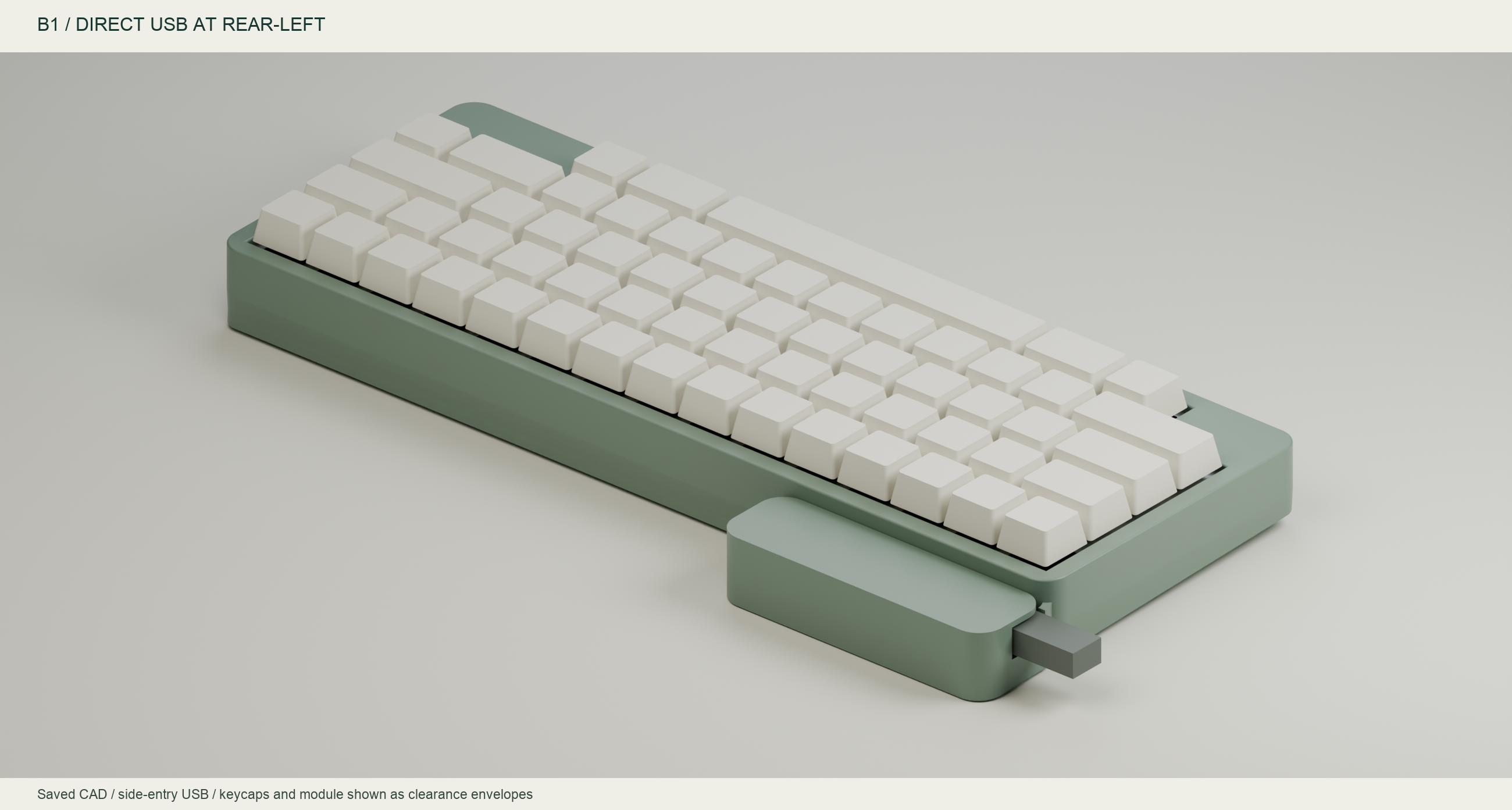
| Item | Current B1.1 definition |
|---|---|
| Layout | 60 keys, HHKB Control position, split right Shift + Fn; left blocker 1.5u, right 2.5u; centered 6u space with 95.25 mm stabilizer spacing |
| Mechanism / plate | NiZ housing, MX-cross slider, silencing ring, separate dome and sensing conical spring; 1.6 mm plate with initial 14.0 mm R0.5 cutouts; qualify in final material |
| Sensing mainboard | Shared A0 four-layer board, 285 × 94.6 × 1.6 mm; no MCU at U1 |
| Daughterboards / FPC | 82 × 24 × 1 mm carrier, 40 × 19 × 1 mm interposer; 24-conductor custom shaped FPC and Molex 200528-0240 connectors |
| Hand assembly | Mainly SOIC, 0805 and through holes; the 1 mm-pitch FPC connectors need flux and magnification; no bare MCU, crystal or RF network assembly |
| Power | Protected 1S, approximately 100 mA default charging, BOOST open; multiple pouches require a factory 1S2P / 1S3P pack with one protection board |
| USB / BLE | Direct to the carrier's nice!nano; Fn+5 selects USB, Fn+6 selects BLE; one reporting endpoint at a time |
| Case | Dedicated B1 base and pod lid with shared A0 HHKB bezel and plate; maximum plan envelope 299 × 136.6 mm, with 28 mm extra depth only at the rear-left pod; no visible top screws |
| Case compatibility | Mainboard mounts reference GH60 / Lot60; the B1 pod is not a universal drop-in fit for commercial GH60 / Poker cases |
B1.1 has 46 populated board/harness positions + one FPC, plus one mainboard-U1 DNP record and 60 unsoldered sensing cells. No per-key diodes, hot-swap sockets, RGB, display or separate USB controller are used.
File entry points:
REFERENCE.Scripts check native electrical reports, selected solid clearances, fabrication ZIPs and render hashes. See reports and the consistency audit for coverage and pending physical tests. File checks do not certify hardware operation.
A0 is the baseline for the shared mainboard, bezel and plate. Its historical workbench, case record, base electrical analysis and battery study are explicitly scoped. The A0 base and incomplete USB extension arrangement are not used by the current B1 assembly.
Original YAKB files use MIT; reused Tako / KiCad library material retains its own licenses. See the source record for attribution boundaries.
| Qty | Value | Footprint | References |
|---|---|---|---|
| 19 | 100k | Resistor_SMD:R_0805_2012Metric_Pad1.20x1.40mm_HandSolder | R10, R11, R12, R13, R14, R15, R16, R17, R18, R19, R20, R21, R22, R23, R24, R30 +3 |
| 5 | 100 | Resistor_SMD:R_0805_2012Metric_Pad1.20x1.40mm_HandSolder | R1, R2, R3, R4, R5 |
| 3 | H_center, H_lower_center, H_upper_left | ||
| 3 | 100n | Capacitor_SMD:C_0805_2012Metric_Pad1.18x1.45mm_HandSolder | C1, C2, C3 |
| 3 | 1k | Resistor_SMD:R_0805_2012Metric_Pad1.20x1.40mm_HandSolder | R31, R32, R36 |
| 2 | CD74HC4051M96 | Package_SO:SOIC-16_3.9x9.9mm_P1.27mm | U2, U3 |
| 1 | ' | YAKB:ecs_pad_1U_no_ring | EC41 |
| 1 | , | YAKB:ecs_pad_1U_no_ring | EC51 |
| 1 | - | YAKB:ecs_pad_1U_no_ring | EC12 |
| 1 | . | YAKB:ecs_pad_1U_no_ring | EC52 |
| 1 | / | YAKB:ecs_pad_1U_no_ring | EC53 |
| 1 | 0 | YAKB:ecs_pad_1U_no_ring | EC11 |
| 1 | 1 | YAKB:ecs_pad_1U_no_ring | EC2 |
| 1 | 1u | Capacitor_SMD:C_0805_2012Metric_Pad1.18x1.45mm_HandSolder | C5 |
| 1 | 2 | YAKB:ecs_pad_1U_no_ring | EC3 |
| 1 | 220p_C0G | Capacitor_SMD:C_0805_2012Metric_Pad1.18x1.45mm_HandSolder | C4 |
| 1 | 3 | YAKB:ecs_pad_1U_no_ring | EC4 |
| 1 | 4 | YAKB:ecs_pad_1U_no_ring | EC5 |
| 1 | 5 | YAKB:ecs_pad_1U_no_ring | EC6 |
| 1 | 6 | YAKB:ecs_pad_1U_no_ring | EC7 |
| 1 | 7 | YAKB:ecs_pad_1U_no_ring | EC8 |
| 1 | 8 | YAKB:ecs_pad_1U_no_ring | EC9 |
| 1 | 9 | YAKB:ecs_pad_1U_no_ring | EC10 |
| 1 | ; | YAKB:ecs_pad_1U_no_ring | EC40 |
| 1 | = | YAKB:ecs_pad_1U_no_ring | EC13 |
| 1 | A | YAKB:ecs_pad_1U_no_ring | EC31 |
| 1 | AO3401A | Package_TO_SOT_SMD:SOT-23 | Q1 |
| 1 | B | YAKB:ecs_pad_1U_no_ring | EC48 |
| 1 | Backspace | YAKB:ecs_pad_1U_no_ring | EC29 |
| 1 | Battery_switch_pigtail | YAKB:SPST_PIGTAIL_2.54 | SW1 |
| 1 | C | YAKB:ecs_pad_1U_no_ring | EC46 |
| 1 | Control | YAKB:ecs_pad_1U_no_ring | EC30 |
| 1 | D | YAKB:ecs_pad_1U_no_ring | EC33 |
| 1 | E | YAKB:ecs_pad_1U_no_ring | EC19 |
| 1 | Enter | YAKB:ecs_pad_1U_no_ring | EC42 |
| 1 | Esc | YAKB:ecs_pad_1U_no_ring | EC1 |
| 1 | F | YAKB:ecs_pad_1U_no_ring | EC34 |
| 1 | Fn | YAKB:ecs_pad_1U_no_ring | EC55 |
| 1 | G | YAKB:ecs_pad_1U_no_ring | EC35 |
| 1 | H | YAKB:ecs_pad_1U_no_ring | EC36 |
| 1 | I | YAKB:ecs_pad_1U_no_ring | EC24 |
| 1 | J | YAKB:ecs_pad_1U_no_ring | EC37 |
| 1 | JST_S2B-PH-K | YAKB:Battery_PH2 | J1 |
| 1 | K | YAKB:ecs_pad_1U_no_ring | EC38 |
| 1 | L | YAKB:ecs_pad_1U_no_ring | EC39 |
| 1 | LAlt | YAKB:ecs_pad_1U_no_ring | EC57 |
| 1 | LGUI | YAKB:ecs_pad_1U_no_ring | EC56 |
| 1 | M | YAKB:ecs_pad_1U_no_ring | EC50 |
| 1 | N | YAKB:ecs_pad_1U_no_ring | EC49 |
| 1 | O | YAKB:ecs_pad_1U_no_ring | EC25 |
| 1 | OPA350UA | Package_SO:SOIC-8_3.9x4.9mm_P1.27mm | U4 |
| 1 | P | YAKB:ecs_pad_1U_no_ring | EC26 |
| 1 | Q | YAKB:ecs_pad_1U_no_ring | EC17 |
| 1 | R | YAKB:ecs_pad_1U_no_ring | EC20 |
| 1 | RAlt | YAKB:ecs_pad_1U_no_ring | EC59 |
| 1 | RGUI | YAKB:ecs_pad_1U_no_ring | EC60 |
| 1 | RShift | YAKB:ecs_pad_1U_no_ring | EC54 |
| 1 | Reset_NO | YAKB:RESET_2.54_TH | SW2 |
| 1 | S | YAKB:ecs_pad_1U_no_ring | EC32 |
| 1 | Shift | YAKB:ecs_pad_1U_no_ring | EC43 |
| 1 | Space | YAKB:ecs_pad_1U_no_ring | EC58 |
| 1 | T | YAKB:ecs_pad_1U_no_ring | EC21 |
| 1 | Tab | YAKB:ecs_pad_1U_no_ring | EC16 |
| 1 | U | YAKB:ecs_pad_1U_no_ring | EC23 |
| 1 | V | YAKB:ecs_pad_1U_no_ring | EC47 |
| 1 | W | YAKB:ecs_pad_1U_no_ring | EC18 |
| 1 | X | YAKB:ecs_pad_1U_no_ring | EC45 |
| 1 | Y | YAKB:ecs_pad_1U_no_ring | EC22 |
| 1 | Z | YAKB:ecs_pad_1U_no_ring | EC44 |
| 1 | [ | YAKB:ecs_pad_1U_no_ring | EC27 |
| 1 | \ | YAKB:ecs_pad_1U_no_ring | EC14 |
| 1 | ] | YAKB:ecs_pad_1U_no_ring | EC28 |
| 1 | ` | YAKB:ecs_pad_1U_no_ring | EC15 |
| 1 | nice!nano_v2 | YAKB:nice_nano | U1 |


SamanHushi/esp_smart_relay_board
Project to conect multiple low power 5V and 12V devices, messure usage and control it with ESPHome


It measures 285 × 94.6 mm and has 4 copper layers, 1.6 mm thick.
103 parts, built around the OPA350UA, CD74HC4051M96 and AO3401A. The full list of its parts is on this page, with links to each part's symbol and footprint where PCBKit's library has them.
From the wZuck/YAKB repository on GitHub, at the commit this page was made from: the board is hardware/YAKB.kicad_pcb and its schematic hardware/YAKB.kicad_sch. PCBKit opens the board in the browser, with nothing to install.
Its repository publishes it under the MIT licence: you may reuse it on that licence's terms (keep the author's notice, and for a copyleft licence share your changes alike).