

2 layers43 × 175 mm

 vruga/esp_medmonitor1
KiCAD project for dual-node ESP32 medical monitoring and security system.
Hackthon PCB is an open-source printed circuit board by vruga, from the vruga/esp_medmonitor repository on GitHub. It is a 2-layer board of 137 × 54.5 mm with 10 parts on 46 nets, routed with 130 tracks and 2 vias.
It is built around the ESP32-C3-DEVKITM-1 and DHT11. Its parts include 5 ICs, 1 resistor and 1 switch. It belongs with the ESP32 and RISC-V boards of this library.
KiCAD project for dual-node ESP32 medical monitoring and security system.
Sensors:
Schematic:
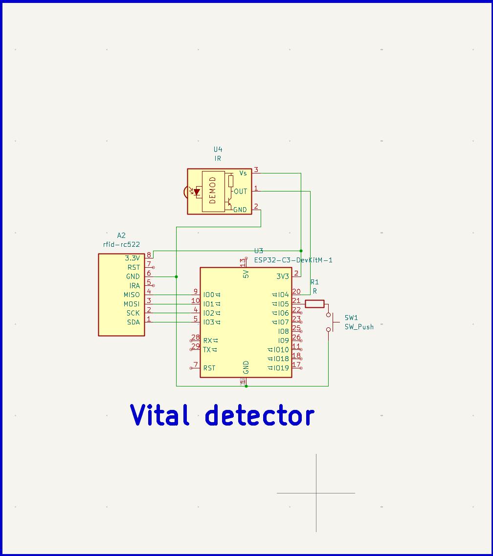
PCB Layout:
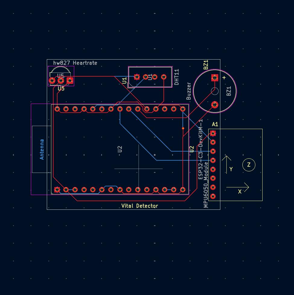
Sensors:
Schematic:
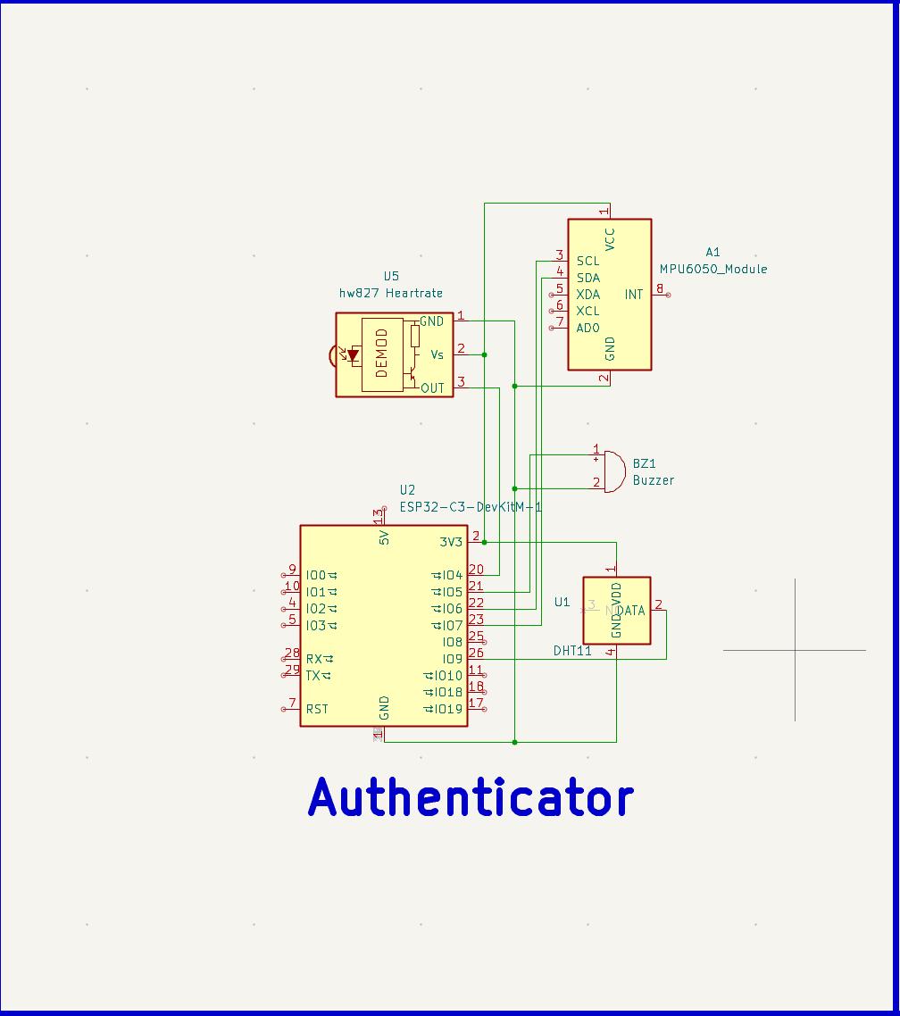
PCB Layout:
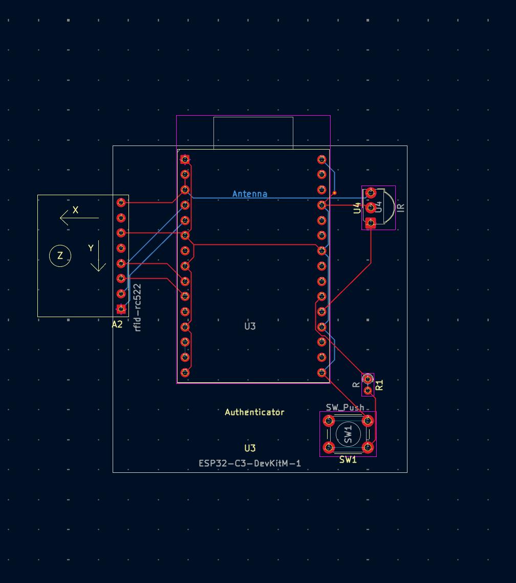
Hackthon_PCB.kicad_pro in KiCAD 8.x+Hackthon_PCB.kicad_schHackthon_PCB.kicad_pcb| Qty | Value | Footprint | References |
|---|---|---|---|
| 2 | ESP32-C3-DevKitM-1 | RF_Module:ESP32-C3-DevKitM-1 | U2, U3 |
| 1 | Buzzer | Buzzer_Beeper:Buzzer_12x9.5RM7.6 | BZ1 |
| 1 | DHT11 | Sensor:Aosong_DHT11_5.5x12.0_P2.54mm | U1 |
| 1 | IR | OptoDevice:Vishay_MOLD-3Pin | U4 |
| 1 | MPU6050_Module | EXTRA_LIB:MPU6050_Module | A1 |
| 1 | R | Resistor_THT:R_Axial_DIN0204_L3.6mm_D1.6mm_P1.90mm_Vertical | R1 |
| 1 | SW_Push | Button_Switch_THT:SW_PUSH_6mm | SW1 |
| 1 | hw827 Heartrate | OptoDevice:Vishay_MOLD-3Pin | U5 |
| 1 | rfid-rc522 | EXTRA_LIB:MPU6050_Module | A2 |
It measures 137 × 54.5 mm and has 2 copper layers, 1.6 mm thick.
10 parts, built around the ESP32-C3-DEVKITM-1 and DHT11. The full list of its parts is on this page, with links to each part's symbol and footprint where PCBKit's library has them.
From the vruga/esp_medmonitor repository on GitHub, at the commit this page was made from: the board is Hackthon_PCB/Hackthon_PCB.kicad_pcb and its schematic Hackthon_PCB/Hackthon_PCB.kicad_sch. PCBKit opens the board in the browser, with nothing to install.
Its repository states no licence, so its author keeps all rights: ask vruga before reusing the design.

Ahmed-YSY/FleetGuard
IoT vehicle telematics for fleet & logistics — ESP32 + SIM7600G 4G/GPS tracker with fuel-theft detection, tamper/cargo security alarms, offline-resilient MQTT reporting, and OBD2 data over ESP-NOW.

iho77/ppo_v2
This work is licensed under a [Creative Commons Attribution-NonCommercial 4.0 International License][cc-by-nc].

TiboDevC/clockclock
Personal project of a kinetic clock inspired by Humans Since 1982, using 48 stepper motors to display time in an artistic and dynamic way.

Abineshpk007/KICAD-solar_panel_monitoring_prototype
This is my PCB, there are many outer like it but this is mine

diaxxu/CNC-Router
a challenge i gave myself to make something great ! yes its a cnc milling / laser / plotter machine

saniyafatima07/Hail_Mary
Lakshya: Low Cost Precision Guidance and Smart Electronic Fuze System
