2 layers27.5 × 69 mm
FlashCore
Omarbelh/FlashCore
Hybrid USB-C SPI Flash & EEPROM programmer based on CH341A and ESP32-S3.
54 parts1MIT

 Upcycle-Electronics/CH341A-Pro81
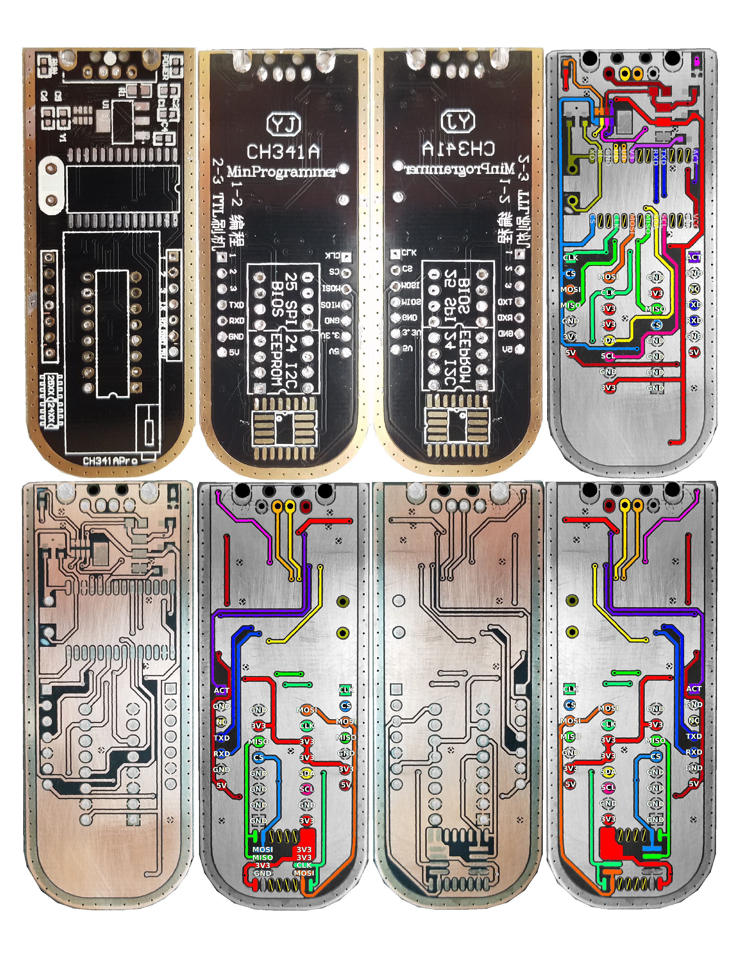
Retrace pics and schematic for the Cheap Black CH341A Serial Flash EEPROM BIOS Programmer
CH341A Pro is an open-source printed circuit board by Upcycle-Electronics, from the Upcycle-Electronics/CH341A-Pro repository on GitHub. It is a 2-layer board of 27.5 × 69 mm with 18 parts on 41 nets, routed with 332 tracks and 107 vias.
It is built around the CH341A and AMS1117-3.3. Its parts include 5 capacitors, 4 ICs, 4 connectors, 2 diodes and 1 resistor. It belongs with the interfaces and adapters boards of this library.


Schematic: https://github.com/Upcycle-Electronics/CH341A-Pro/blob/master/ch341Apro_schematicV01.pdf
| Qty | Value | Footprint | References |
|---|---|---|---|
| 2 | 104 | Capacitor_SMD:C_0603_1608Metric | C1, C2 |
| 2 | 20p | Capacitor_SMD:C_0603_1608Metric | C5, C6 |
| 2 | Conn_01x07 | Connector_PinSocket_2.54mm:PinSocket_1x07_P2.54mm_Vertical | J2, J4 |
| 1 | 0R | Resistor_SMD:R_0805_2012Metric | R1 |
| 1 | 12M | Crystal:Crystal_HC49-U_Vertical | Y1 |
| 1 | 222 | Resistor_SMD:R_Array_Convex_4x0603 | RN1 |
| 1 | 472 | Capacitor_SMD:C_0603_1608Metric | C4 |
| 1 | AMS1117-3.3 | Package_TO_SOT_SMD:SOT-223-3_TabPin2 | U1 |
| 1 | CH341a | Package_SO:SOIC-28W_7.5x17.9mm_P1.27mm | U2 |
| 1 | I2C EEPROM | Package_SO:SOIC-8_3.9x4.9mm_P1.27mm | U4 |
| 1 | Power | LED_SMD:LED_0603_1608Metric | D1 |
| 1 | RUN | LED_SMD:LED_0603_1608Metric | D2 |
| 1 | SPI FLASH | Package_SO:SOIC-16W_7.5x10.3mm_P1.27mm | U3 |
| 1 | USB_A | connectors:USB_A_MALE_Generic | J1 |
| 1 | ZIF-16 | Socket:DIP_Socket-16_W4.3_W5.08_W7.62_W10.16_W10.9_3M_216-3340-00-0602J | J3 |
It measures 27.5 × 69 mm and has 2 copper layers, 1.6 mm thick.
18 parts, built around the CH341A and AMS1117-3.3. The full list of its parts is on this page, with links to each part's symbol and footprint where PCBKit's library has them.
From the Upcycle-Electronics/CH341A-Pro repository on GitHub, at the commit this page was made from: the board is CH341Apro.kicad_pcb. PCBKit opens the board in the browser, with nothing to install.
Its repository states no licence, so its author keeps all rights: ask Upcycle-Electronics before reusing the design.
Omarbelh/FlashCore
Hybrid USB-C SPI Flash & EEPROM programmer based on CH341A and ESP32-S3.

ADBeta/CH341A_USB_C
USB-C CH341A Breakout Board with EEPROM, I2C, SPI and UART Outputs - with headers for SOIC Clips


AliceAch/SPIN-FV1-Tone-Dev
A PCB Tone Development board for Guitar Effects, built around the SPIN FV1 DSP IC.

CatspersCoffee/S100-Boards
S-100 bus boards designed and built: Z80 and 80386 CPU cards, SRAM/DRAM memory, CPLD/FPGA I/O and SPI boards, an 18-slot backplane and bus terminator.


