
2 layers138.1 × 114.3 mm

One 2-layer board under the plate that replaces the plate's handwiring: rows, columns, diodes, power buses and screen jumpers. Fits the printed parts as they are: no plate, frame, dock or lid reprint.
Deck is an open-source printed circuit board by unbleavabl, from the unbleavabl/deck-macropad repository on GitHub. It is a 2-layer board of 169.2 × 105 mm with 67 parts on 41 nets, routed with 589 tracks and 11 vias.
Its parts include 17 switches, 14 diodes and 3 capacitors.
One 2-layer board under the plate that replaces the plate's handwiring: rows, columns, diodes, power buses and screen jumpers. Fits the printed parts as they are: no plate, frame, dock or lid reprint. Same pins as the handwired build, so the firmware doesn't change.
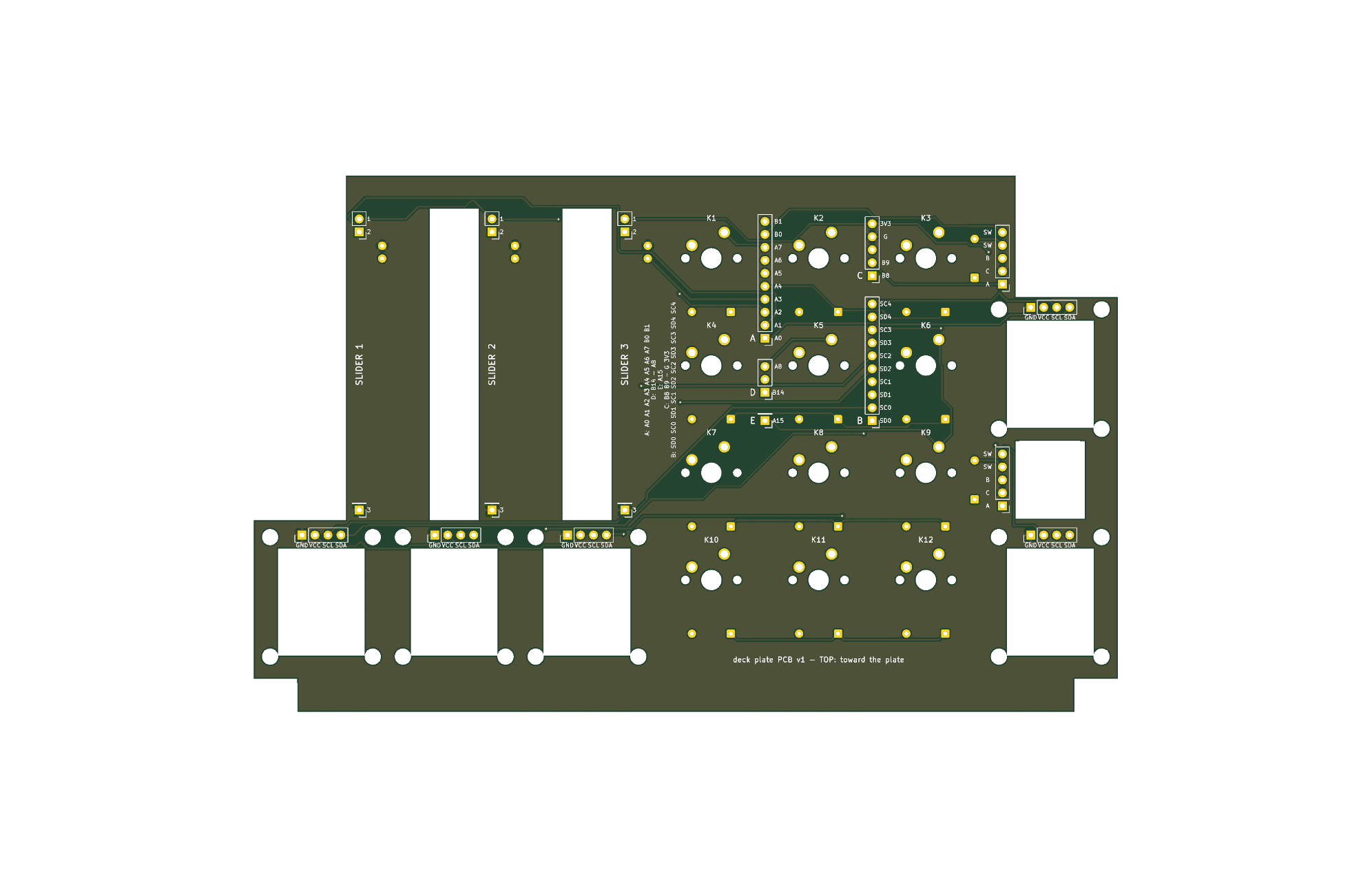
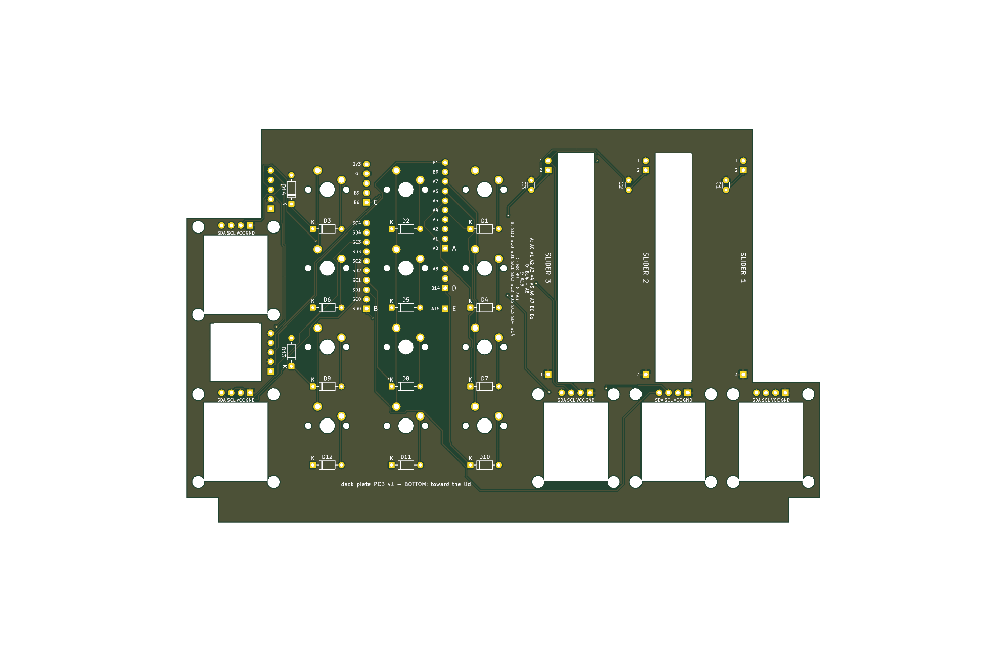
1 (3V3) and 2 (wiper); pin 3 at the front end, pad 3 (GND). The 100 nF cap is on the board (C1-C3).A C B SW SW (A, C, B = the 3-pin side; the two SW pads take the two push pins, either way round). The push diode is on the board (D13, D14).| Ref | Part | Side |
|---|---|---|
| K1-K12 | MX switch (3- or 5-pin) | top, through the plate |
| D1-D14 | 1N4148, through-hole | bottom; band (square pad, K) toward the row |
| C1-C3 | 100 nF ceramic, 2.5 mm pitch | bottom |
| S1-S5 | the screens' own pins | top |
| JA-JE | harness wires (or 2.54 male headers) | from the bottom |
| J_P*, J_E* | pot / encoder lead pads | wires from the bottom |
wiring/wiring.html's checklist.Upload deck-gerbers.zip. It's 169.3 x 105.1 mm, 2 layers, 1.6 mm, HASL, any colour. Over 100 mm, so the $2 price doesn't apply. Rules used: 0.25 mm tracks (a few necked to 0.15 at pads), 0.25 mm clearance, 0.35 mm via drill, GND pour on both layers.
Before ordering: print fit-check-1to1.pdf at 100 % (no "fit to page"), check a key's 14 mm square measures 14 mm, cut out the outline, and hold it under the plate. Every switch, peg, pot slot and encoder hole should line up.
./route.sh runs the whole thing: build_pcb.py places parts from the deck geometry (mirrors case/scad/deck.scad; change sizes there and here together), freerouting autoroutes, then GND pour, DRC (drc.rpt, must be clean), Gerbers, renders and the fit-check PDF. Needs KiCad 10 (pacman -S kicad kicad-library), Java 25 (mise install java@temurin-25) and freerouting-2.5.0.jar in ~/.cache/freerouting/ (GitHub releases). deck.kicad_pcb opens in KiCad for hand edits, but route.sh overwrites it.
| Qty | Value | Footprint | References |
|---|---|---|---|
| 20 | peg | deck:PegHole_3.2mm | H1LB, H1LF, H1RB, H1RF, H2LB, H2LF, H2RB, H2RF, H3LB, H3LF, H3RB, H3RF, H4LB, H4LF, H4RB, H4RF +4 |
| 14 | 1N4148 | D_DO-35_SOD27_P7.62mm_Horizontal | D1, D2, D3, D4, D5, D6, D7, D8, D9, D10, D11, D12, D13, D14 |
| 12 | MX | SW_Cherry_MX_1.00u_PCB | K1, K2, K3, K4, K5, K6, K7, K8, K9, K10, K11, K12 |
| 5 | PinHeader_1x04_P2.54mm_Vertical | PinHeader_1x04_P2.54mm_Vertical | S1, S2, S3, S4, S5 |
| 4 | PinHeader_1x01_P2.54mm_Vertical | PinHeader_1x01_P2.54mm_Vertical | J_P1G, J_P2G, J_P3G, JE |
| 3 | 100n | C_Disc_D3.0mm_W1.6mm_P2.50mm | C1, C2, C3 |
| 3 | PinHeader_1x02_P2.54mm_Vertical | PinHeader_1x02_P2.54mm_Vertical | J_P1, J_P2, J_P3 |
| 3 | PinHeader_1x05_P2.54mm_Vertical | PinHeader_1x05_P2.54mm_Vertical | J_E1, J_E2, JC |
| 2 | PinHeader_1x10_P2.54mm_Vertical | PinHeader_1x10_P2.54mm_Vertical | JA, JB |
| 1 | PinHeader_1x03_P2.54mm_Vertical | PinHeader_1x03_P2.54mm_Vertical | JD |
It measures 169.2 × 105 mm and has 2 copper layers, 1.6 mm thick.
67 parts. The full list of its parts is on this page, with links to each part's symbol and footprint where PCBKit's library has them.
From the unbleavabl/deck-macropad repository on GitHub, at the commit this page was made from: the board is macropad/pcb/deck.kicad_pcb. PCBKit opens the board in the browser, with nothing to install.
Its repository states no licence, so its author keeps all rights: ask unbleavabl before reusing the design.


Ardumower/ardumower
Develop an open source robotic lawn mower (HW+SW reference platform)

CRImier/MyKiCad
My KiCad boards. Can't be bothered uploading individually anymore, so here you go.


