2 layers65.4 × 62.1 mm
OBJEX EHDK v1.0
salvatoreraccardi/Energy-Harvesting-DevKit
OBJEX EHDK - Energy harvesting DevKit
106 parts22

 tux2603/watch2
A simple, ATtiny402 powered binary wrist watch. Sponsored by PCBWay
Watch is an open-source printed circuit board by tux2603, from the tux2603/watch repository on GitHub. It is a 2-layer board of 2 × 27.5 mm with 27 parts on 14 nets, routed with 160 tracks and 13 vias.
It is built around the ATTINY402-SSN and BAT-HLD-001-TR. Its parts include 12 diodes, 7 resistors, 2 switches and 1 IC. It belongs with the wearables boards and the AVR (ATmega, ATtiny) boards of this library.

revision 2.0
A 12 hour wrist watch that displays the current time in BCD using LEDs. The watch is powered by a single CR2032 coin cell and uses an ATtiny402 microcontroller to keep track of time and drive the LEDs. The time can be viewed or set at any time by pressing the two buttons on the face of the watch.
PCB fabrication for this project was sponsered by PCBWay, and I would like to thank them for their support! I was very happy with the quality of the PCBs they sent me, and their staff was very easy to work with.
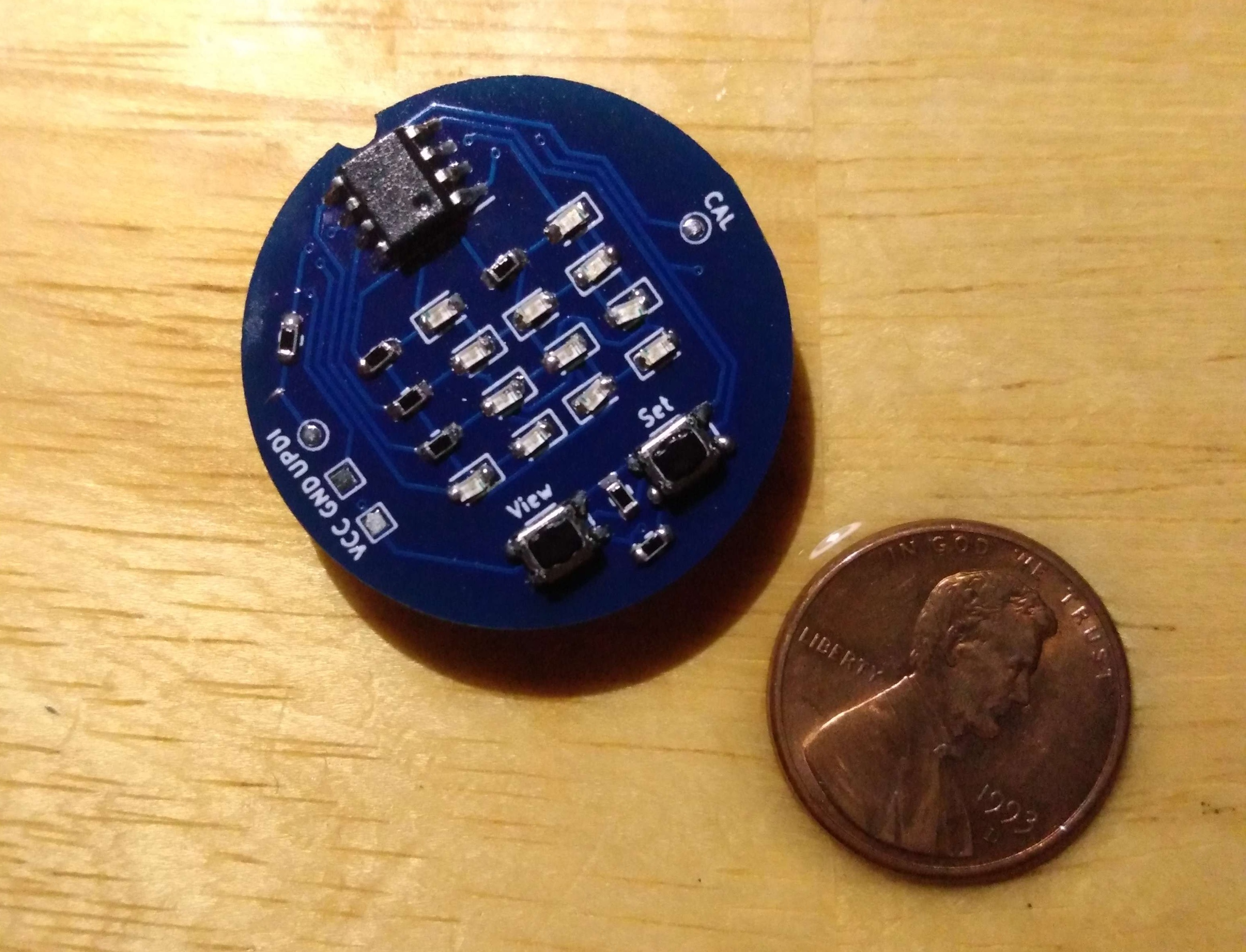
Fully assembled PCB, supplied by PCBWay and hand assembled by me. US penny for scale
To view the time, simply press the VIEW button on the face of the watch. This will automatically wake the microcontroller and display the current time for 10 seconds. After 10 seconds, the LEDs will be turned off and the microcontroller will go back to sleep, conserving battery life.
To set the time, first wake the watch from sleep by pressing the VIEW button. Once the watch is awake, press the SET button. The watch will now be in time setting mode, and the digit that is currently selected will flash once every two seconds. To change the value of the currently selected digit, press the VIEW button. Once the desired value is entered, press the SET button again to select the next digit and repeat until all digits are set. Once all digits are set, the watch will automatically return to view mode and go back to sleep after 10 seconds.
To reset the watch, first wake the watch from sleep by pressing the VIEW button. Once the watch is awake, press and hold either button for at least three seconds. The watch will save the currently set time before resetting and will automatically return to view mode after the reset is complete.
Some trickery was needed to drive twelve LEDs and read two push buttons with the limited number of GPIO pins available. The LEDs are arranged in a charlieplexing matrix, allowing all twelve LEDs to be controlled with just four tri-state GPIO pins. The push buttons are then read using a small resistor ladder with a single GPIO pin. Pressing the VIEW button will pull the voltage on the pin to GND, and pressing the SET button will pull the voltage on the pin to 0.5 * Vdd. If no button is pressed, the voltage on the pin is pulled to Vdd. This way, only five GPIO pins are used and PA0 is left to function solely as the UPDI pin, allowing for easy programming of the ATtiny402.
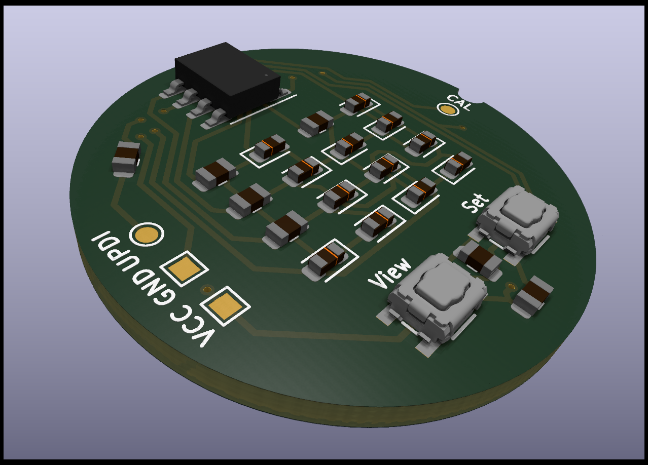
| Description | Count | Manufacturer Part Number | DigiKey Part Number | Substitutions |
|---|---|---|---|---|
| CR2032 coin cell holder | 1 | BAT-HLD-001-TR | BAT-HLD-001-TRCT-ND | Substitutions are possible, but will require traces to be re-routed |
| Blue LED | 12 | IN-S63BT5B | 1830-1068-1-ND | Any other 0603 LED can be used, but if a different color is used the color will be different |
| 47Ω 1/8W Resistor | 4 | ERJ-H3GJ470V | 10-ERJ-H3GJ470VCT-ND | Any 0603, 47Ω resistor with a power rating of 1/8W or higher |
| 4.7kΩ 1/8W Resistor | 1 | ERJ-H3GJ472V | 10-ERJ-H3GJ472VCT-ND | Any 0603, 4.7kΩ resistor with a power rating of 1/8W or higher |
| 10kΩ 1/8W Resistor | 2 | ERJ-H3GJ103V | 10-ERJ-H3GJ103VCT-ND | Any 0603, 4.7kΩ resistor with a power rating of 1/8W or higher |
| Momentary switch | 2 | EVP-AA202K | P13348SCT-ND | Substitutions are possible, but will require traces to be re-routed |
| ATtiny 402 microcontroller | 1 | ATTINY402-SSNR | ATTINY402-SSNRCT-ND | Any ATtiny402. The ATtiny202 should also work, but has less flash and has not been tested. |
| Description | Count | Source |
|---|---|---|
| Watch Body | 1 | CAD file |
| Watch Back | 1 | CAD file |
| PCB | 1 | Gerber files |
| CR2032 coin cell | 1 | Your favorite source for watch batteries |
| 18mm watch band | 1 | Your favorite source for watch bands |
Unless you're lucky enough to have PCB fabrication facilities in house, you'll need to send the Gerber files to a third-party manufacturer for fabrication. I used DKRed for my initial prototypes, but after releasing v1 PCBWay reached out to me and offered to sponsor PCB fabrication for v2. Since I had selected tolerances to work with all of the major PCB fabrication services, I was more than happy to accept their offer. Having worked with both DKRed's ENIG finish and PCBWay's HASL finish, I would definietly have to say I preffered PCBWay's HASL for hand-soldering. The HASL finish made the soldering process a little bit easier, which when you're hand soldering small SMD components is always appreciated.
The components for the watch were picked to make hand soldering possible with a decent soldering iron and a steady hand, but it should also be possible to use a reflow oven or hot plate to solder the components on the face of the PCB. The battery holder will still likely need to be soldered by hand though, but it's nice and big so it shouldn't be too difficult. For hand soldering, I used the following procedure:
Solder the LEDs and 47Ω resistors to the middle section of the PCB.
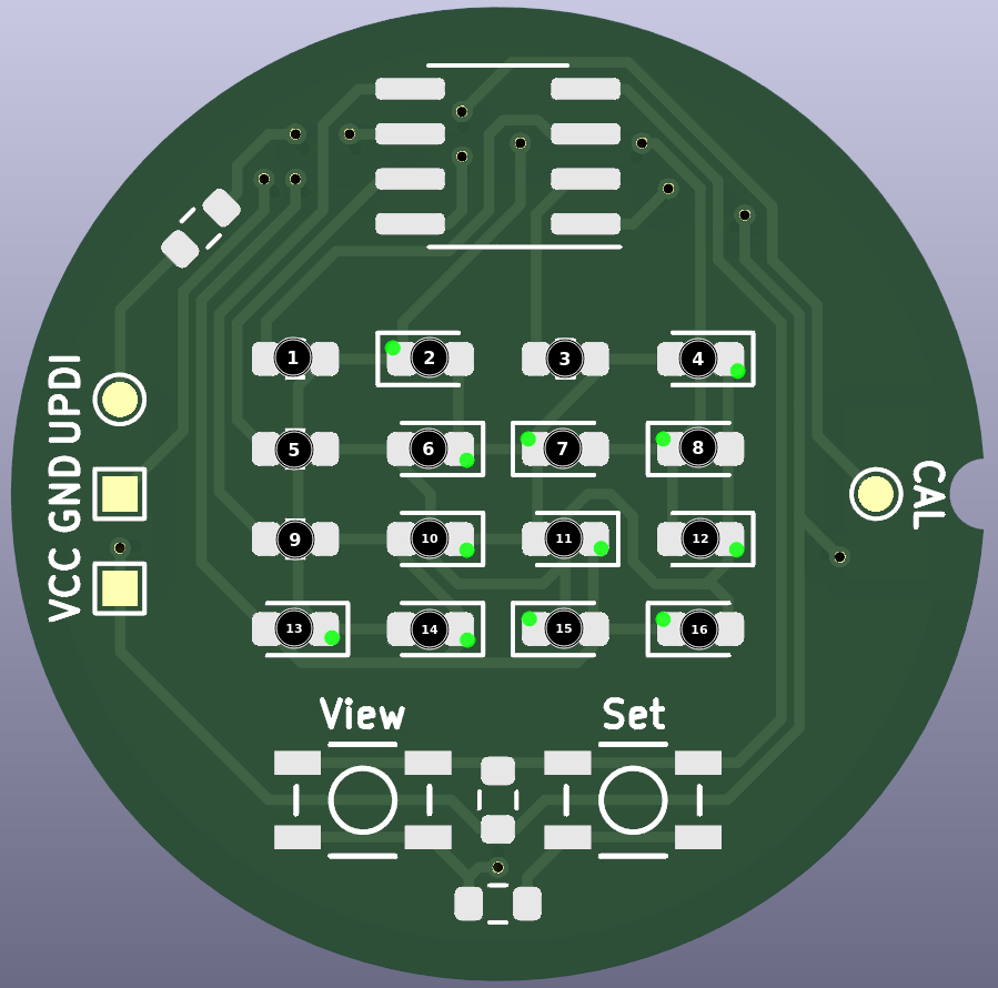
Figure 1: LED and resistor placement
Verify that the resistors and LEDs were placed correctly
| LED | Positive pad | Negative pad |
|---|---|---|
| 2 | 1 | 2 |
| 4 | 1 | 3 |
| 6 | 3 | 1 |
| 7 | 2 | 1 |
| 8 | 3 | 2 |
| 10 | 4 | 1 |
| 11 | 1 | 4 |
| 12 | 2 | 3 |
| 13 | 4 | 2 |
| 14 | 2 | 4 |
| 15 | 4 | 3 |
| 16 | 3 | 4 |
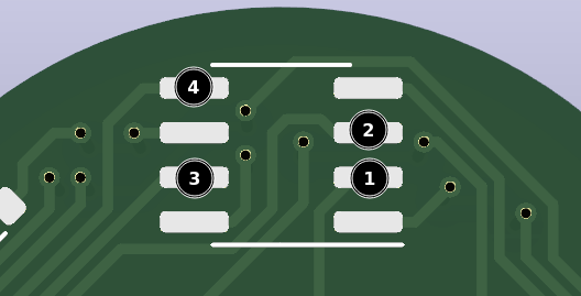
Figure 2: LED test pads
Solder the 4.7kΩ an 10kΩ resistors to the PCB
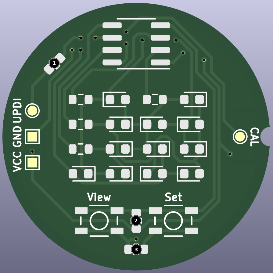
Figure 3: Remaining resistor placement
Solder the buttons to the PCB
SW1 and SW2. The buttons aren't polarized, so they can be soldered in either directionSolder the ATtiny402 to the PCB
Solder the battery holder to the PCB
Three solder pads, labeled VCC, GND, and UPDI, are supplied on the watch face to allow for simple programming of the ATtiny using a UPDI programmer. Any UPDI programmer should work, but I used an Arduino Uno running jtag2updi. The 4.7k series resistor required for flashing is already included on the PCB, so no external resistor is necessary.
Connect the VCC, GND, and UPDI solder pads to the corresponding pins using jumper wires. These jumper wires can be soldered or clipped on, it doesn't really matter. Note that the pads and traces are very small and fragile, so be careful not to put too much stress on them or they could rip off of the PCB.
Hook the Arduino up to your PC and note what port it is connected to (eg, COM3, /dev/ttyACM0, /dev/ttyUSB0, etc). Set the PORT variable on line four of the Makefile to this value, replacing the default value of /dev/ttyACM0
Run make flash to flash the watch. Alternatively, you can manually run the command avrdude -c jtag2updi -P <YOUR_PORT> -p attiny402 -U flash:w:bin/main.hex -U eeprom:w:bin/eeprom.hex to flash the watch.
The watch should automatically enter calibration mode after flashing. If you don't want to calibrate the watch right now, just hold down the VIEW button for at least three seconds to reset the watch.
After flashing the firmware, the watch will automatically enter one-time calibration mode. In this mode the watch will generate a square wave on the CAL solder pad, which can be measured using an oscilloscope. The period of this waveform should be as close to 468.75ms as possible, but it will initially be a good deal off from this value. To calibrate the watch, follow these steps:
CAL solder pad to the positive terminal of an oscilloscope probe using a jumper wire. Connect the negative terminal of the probe to the GND solder pad.VIEW button to decrease the period.SET button to increase the period.To prevent accidental re-calibration, the watch will only enter calibration mode immediately after flashing by default. If you want to enable entering calibration mode without flashing the watch, write the value 0x01 to EEPROM address 0x05. This will allow the watch to enter calibration mode by holding down the SET button for at least three seconds. To disable this feature again, write the value 0x00 to EEPROM address 0x05.
The functionality of the watch can be customized by modifying, compiling, and flashing the source code. For simple changes, the following configuration options can be modified in the config.h file:
| Option | Description | Default Value | Recommended Range | Units |
|---|---|---|---|---|
BLINK_FREQUENCY | The frequency at which the currently selected digit will blink while in time setting mode | 1 | 0.25 - 2 | Hz |
DEBOUNCE_COUNT | The number of consecutive update cycles that a button state must be stable before it is considered to be pressed | 50 | 5 - 500 | update cycles |
RESET_HOLD_TIME | The number of seconds that a button must be held before the watch is reset | 3 | 1 - 10 | s |
SLEEP_TIMEOUT | The number of seconds that the watch will remain awake before automatically going back to sleep | 10 | 1 - 60 | s |
UPDATE_FREQUENCY | The frequency at which the LED matrix is updated and input is read from the buttons. | 480 | 96 - 5000 | Hz |
To compile the code, the avr-gcc tool chain will need to be installed with support for the ATtiny402
This work is licensed under a Creative Commons Attribution-NonCommercial 4.0 International License. You are free to share, use, and modify this work for any non-commercial reasons as long as you give appropriate credit. The author grants permission for PCB and CAD design files to be sent to third-party manufacturers for fabrication as long as these fabricated parts or assemblies containing these fabricated parts are not later resold for profit.
| Qty | Value | Footprint | References |
|---|---|---|---|
| 12 | LED_Small | LED_SMD:LED_0603_1608Metric | D1, D2, D3, D4, D5, D6, D7, D8, D9, D10, D11, D12 |
| 4 | 47 Ω | Resistor_SMD:R_0603_1608Metric | R1, R2, R3, R4 |
| 3 | 4.7 kΩ | Resistor_SMD:R_0603_1608Metric | R5, R6, R7 |
| 2 | EVP-AA202K | Push Button:SW_EVP-AA102K_PAN | SW1, SW2 |
| 2 | TestPoint | TestPoint:TestPoint_Pad_D1.0mm | TP1, TP4 |
| 2 | TestPoint | TestPoint:TestPoint_Pad_1.0x1.0mm | TP2, TP3 |
| 1 | ATtiny402-SS | Package_SO:SOIC-8_3.9x4.9mm_P1.27mm | U1 |
| 1 | BAT-HLD-001-TR | Battery Holder:BAT_BAT-HLD-001-TR | BT1 |
It measures 2 × 27.5 mm and has 2 copper layers, 1.6 mm thick.
27 parts, built around the ATTINY402-SSN and BAT-HLD-001-TR. The full list of its parts is on this page, with links to each part's symbol and footprint where PCBKit's library has them.
From the tux2603/watch repository on GitHub, at the commit this page was made from: the board is pcb/watch.kicad_pcb and its schematic pcb/watch.kicad_sch. PCBKit opens the board in the browser, with nothing to install.
Its repository states no licence, so its author keeps all rights: ask tux2603 before reusing the design.
salvatoreraccardi/Energy-Harvesting-DevKit
OBJEX EHDK - Energy harvesting DevKit


GoodByte-Hardware/BTZ-EndDevice
Low-power wireless sensor board based on the nRF54L15 for BLE Mesh, Thread/Matter and Zigbee


unicab369/ESP-MESS
I am building a Wireless Bridge System that can manage multiple devices using a variety of wireless technologies.


PocketConcepts/Pocket_PSU
A variable current & voltage PSU with 3S lipo charging, balancing, and protection circuit using PPS.

k-takata/PCB_avr_dx_unbricker
UPDI High Voltage programmer for AVR Dx/Ex series