4 layers78 × 46.3 mm

 TUDA-MUST/Multi-Ferro-DAQ
Measurement Setup to analyze multiple ferroelectric sensors simultaneously
Multi Ferro DAQ is an open-source printed circuit board by TUDA-MUST, from the TUDA-MUST/Multi-Ferro-DAQ repository on GitHub. It is a 4-layer board of 50 × 65 mm with 149 parts on 127 nets, routed with 1,107 tracks and 277 vias.
It is built around the ESP32-S3-MINI-1-N8, ADS131E08IPAGR and LM2775QDSGRQ1, with the AD8608ARUZ-REEL, ICM-42670-P and TP4056 among its other parts. Its parts include 21 resistors, 16 capacitors, 10 ICs, 7 connectors and 6 diodes. It belongs with the sensors and measurement boards and the ESP32 boards of this library.


Wearable 8-channel charge amplifier and data acquisition system for piezo- and ferroelectric sensors.
The system reads up to 8 charge sources simultaneously via two RJ45 connectors (4 sensors per connector). The PCB is designed for mobile use: it can be strapped to a test person, runs on battery power, and streams data in millivolts (mV) via Wi-Fi at up to 2000 samples per second.
| Parameter | Value |
|---|---|
| Channels | 8, simultaneously sampled |
| ADC | TI ADS131E08, 24 bit ΔΣ, programmable gain G = 1, 2, 4, 8, 12 |
| Charge amplifier | AD8608 (quad CMOS op-amp), one per channel |
| Feedback network | C_F = 680 pF (C0G, ±5 %) ∥ R_F = 1 GΩ (±10 %) |
| Sensitivity | 1 / C_F ≈ 1.47 mV/pC |
| Time constant / lower cut-off | τ = R_F · C_F = 0.68 s → f_c = 1 / (2π τ) ≈ 0.23 Hz |
| Output range (vs. V_bias) | ±2.5 V at G = 1, ±4 V / G for G ≥ 2 |
| Charge range | ±1.70 nC at G = 1 (fault flag above ±2.375 V ≈ ±1.62 nC) |
| Sample rate | 1–2 kSa/s recommended (ADC supports up to 64 kSa/s, but samples are lost above 2 kSa/s) |
| Microcontroller | ESP32-S3-MINI-1-N8 |
| Data interface | Wi-Fi 2.4 GHz access point, TCP port 8080 |
| Power | 1S Li-ion/LiPo (protected cell, JST-PH) or USB-C; on-board charger ≈ 336 mA |
| On-board supplies | 5 V analog (LM2775 charge pump), 3.3 V digital (TPS7A91 LDO), V_bias = 2.5 V |
| Extras | 6-axis IMU (ICM-42670-P), 2 RGB status LEDs, board-level RF shield over the analog front end |
| PCB | 4 layers, 50 mm × 65 mm |
flowchart LR
    S["Sensors<br/>2 × RJ45, 4 each"] --> CA["8 × charge amplifier<br/>AD8608<br/>C_F = 680 pF ∥ R_F = 1 GΩ"]
    VB["V_bias = 2.5 V<br/>TLV9051 buffer"] --> CA
    VB --> ADC
    CA --> ADC["ADS131E08<br/>8 ch, 24 bit, simultaneous"]
    ADC -- "SPI + DRDY" --> MCU["ESP32-S3"]
    MCU -- "Wi-Fi, TCP :8080" --> PC["Client<br/>MATLAB / MMM"]
    IMU["IMU ICM-42670-P"] -.-> MCU
Analog front end. The board runs from a single 5 V analog supply. To process bipolar charge signals, all analog circuitry is referenced to a mid-supply voltage V_bias = 2.5 V. V_bias is generated by the ADS131E08's internal op-amp and buffered by a TLV9051. Each channel is an inverting charge amplifier: the non-inverting input is tied to V_bias, the inverting input is the summing node the sensor connects to, and C_F ∥ R_F form the feedback. R_F provides the DC path that keeps the output from drifting, and sets the lower cut-off frequency.
Digitization. The ADS131E08 samples all eight amplifier outputs simultaneously and measures each one differentially against V_bias, so the result is the amplifier's output voltage relative to mid-supply. The analog front end and the ADC sit under a board-level RF shield.
Firmware. The ESP32-S3 uses both cores. An interrupt on the ADC's DRDY signal reads each sample into a queue. A second task converts the raw values to mV, removes the selected PGA gain, and sends packets of 64 samples to the client over TCP.
Power. The board runs from a 1S Li-ion/LiPo cell or USB-C. A TP4056 charges the cell from USB. An LM2775 charge pump supplies the 5 V analog rail, and a TPS7A91 low-noise LDO supplies the 3.3 V digital rail.
The firmware streams each channel as the amplifier output voltage U (in mV, relative to V_bias, with the PGA gain already removed). For signal frequencies well above the cut-off f_c ≈ 0.23 Hz, the charge Q delivered by the sensor into the amplifier input is
$$Q = -C_F \cdot U$$
With C_F = 680 pF:
$$Q,[\mathrm{pC}] = -0.68 \cdot U,[\mathrm{mV}]$$
Example: U = 100 mV → Q = −68 pC. The amplifier is inverting, so the sign of the output is opposite to the sign of the charge flowing into the input.
The feedback resistor makes the amplifier a high-pass. A charge step decays as e^(−t/τ) with τ = 0.68 s: after 0.68 s only 37 % of the step remains, and after 3.4 s (5τ) less than 1 %. For slow or quasi-static signals, correct for this with the transfer function
$$H(f) = -\frac{1}{C_F} \cdot \frac{j 2\pi f \tau}{1 + j 2\pi f \tau}$$
Each RJ45 port carries four sensors. Each sensor uses one wire pair: one pin goes to the amplifier input (signal), the other to V_bias. Pin numbers follow the jack; wire colors follow the T-568B standard.
| Pair | Signal pin | V_bias pin | Signal wire / V_bias wire (T-568B) | Port I | Port II |
|---|---|---|---|---|---|
| A | 5 | 4 | white-blue / blue | IN4 | IN8 |
| B | 2 | 1 | orange / white-orange | IN3 | IN7 |
| C | 6 | 3 | green / white-green | IN2 | IN6 |
| D | 8 | 7 | brown / white-brown | IN1 | IN5 |
INx corresponds to CHANx in the data stream.
Important: the V_bias pins sit at 2.5 V above board ground. Never connect them to GND or to the cable shield. Shorting V_bias to ground loads the reference and drives the channels into saturation. Use the RJ45 shield for the cable screen. It connects to the board's shield net.
The pinout is also printed on the PCB silkscreen.
PCB/jlcpcb/production_files: Gerber archive, BOM and CPL.
PCB/jlcpcb/Added Info.txt).The complete bill of materials, with manufacturer part numbers, key specs and datasheet links, is in PCB/BOM (CSV). The design files require KiCad 9. All project-specific symbols, footprints and 3D models are in PCB/components.
The ESP32-S3 is flashed with the Arduino IDE using
Software/ADC_readout/ardu_adc_dual_core_wifi_tcp/ardu_adc_dual_core_wifi_tcp.ino.
The sketch includes the driver from Software/ADC_readout/lib/, so keep the folder structure intact.
Required:
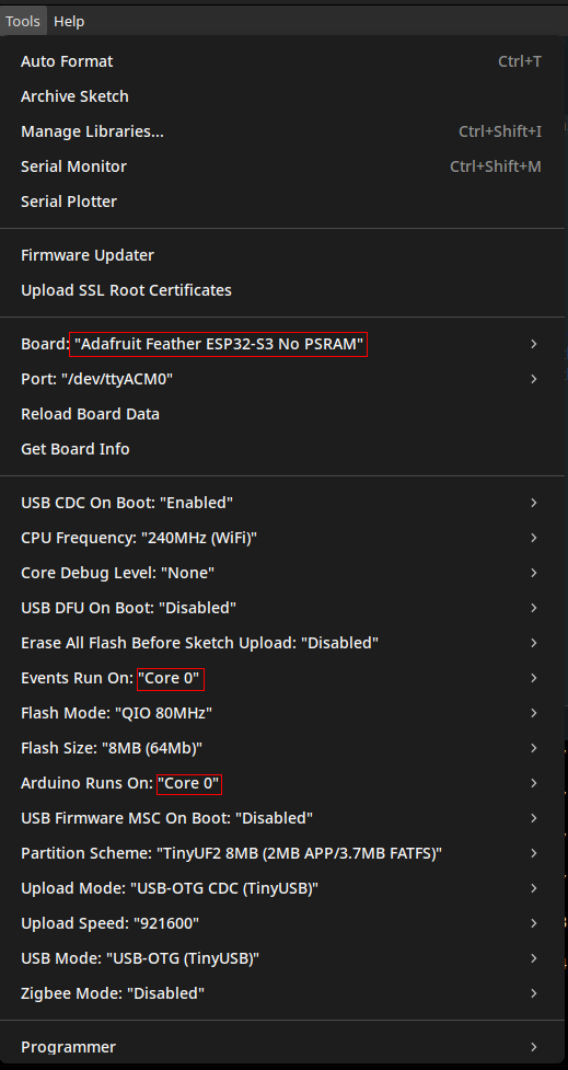
Board settings (Tools menu):
| Setting | Value |
|---|---|
| Board | Adafruit Feather ESP32-S3 No PSRAM |
| USB CDC On Boot | Enabled |
| CPU Frequency | 240 MHz (WiFi) |
| Events Run On | Core 0 |
| Arduino Runs On | Core 0 |
| Flash Mode | QIO 80 MHz |
| Flash Size | 8 MB (64 Mb) |
| Partition Scheme | TinyUF2 8MB (2MB APP/3.7MB FATFS) |
| Upload Mode | USB-OTG CDC (TinyUSB) |
| USB Mode | USB-OTG (TinyUSB) |
For the first flash, or if the upload fails, put the ESP32 into programming mode: press and hold BOOT, briefly press RESET, then release BOOT. The ESP32 is then detected automatically, or can be selected as an "ESP32 Family Device" under the port selection.
Only enter programming mode after a compile/upload for the board above has started. Otherwise the IDE tries, and fails, to build for an "ESP32 Family Device".
The firmware is tested with the MATLAB script Software/ADC_readout/Matlab/ADC_WiFi_readout_TCP.m using MATLAB R2024b.
Connect to the ESP32's Wi-Fi hotspot:
ESP32_Hotspot123456789Then connect to IP address 192.168.4.1 on TCP port 8080 (see this MATLAB script for details).
The hotspot credentials are hard-coded in the firmware. Change them in the sketch if the board is used outside the lab.
The ESP32 expects initialization values in a fixed format and order (36 bytes, little-endian). Garbage bytes can be sent to initialize with the ADC's own default values.
| Data Type | Count | Description |
|---|---|---|
int64 | 1 | Maximum number of samples to collect (PCB resets afterwards). |
uint32 | 1 | ADC sample rate. Choose from 1000, 2000, 4000, 8000, 16000, 32000, 64000. Rates above 2000 cause sample loss and are not recommended. |
uint16 | 8 | ADC settings registers for CHAN1–CHAN8. Only the lower byte is used; set the upper byte to zero. |
uint8 | 8 | PGA gain for CHAN1–CHAN8 (1, 2, 4, 8 or 12). These overwrite the gain previously set in the settings registers. The microcontroller removes the gain before transmitting the data. |
Once initialized, the status LED turns GREEN. It stays green until:
Battery indicator LED:
After setup, the microcontroller sends data via TCP to the client until:
The TCP stream consists of samples of nine little-endian float32 values (36 bytes per sample), sent in packets of 64 samples (2304 bytes):
| Channel | Description |
|---|---|
| CHAN1–CHAN8 | Amplifier output in mV relative to V_bias (–2500 mV to +2500 mV). See Converting the output to charge. |
| CHAN9 | Timestamp in µs since the last ESP32 reset |
Fault Flags:
–9999 mV or +9999 mV means the ADC's negative or positive fault flag was triggered.
This happens when the measured value exceeds ±2375 mV (≈ 95 % of the input range).Timestamp resolution: the timestamp is transmitted as float32, so its resolution decreases with time since reset. The step size is 2 µs after 16.8 s, 64 µs after 9 min, and 512 µs after 71.6 min. Reset the board before long measurements if exact sample timing matters.
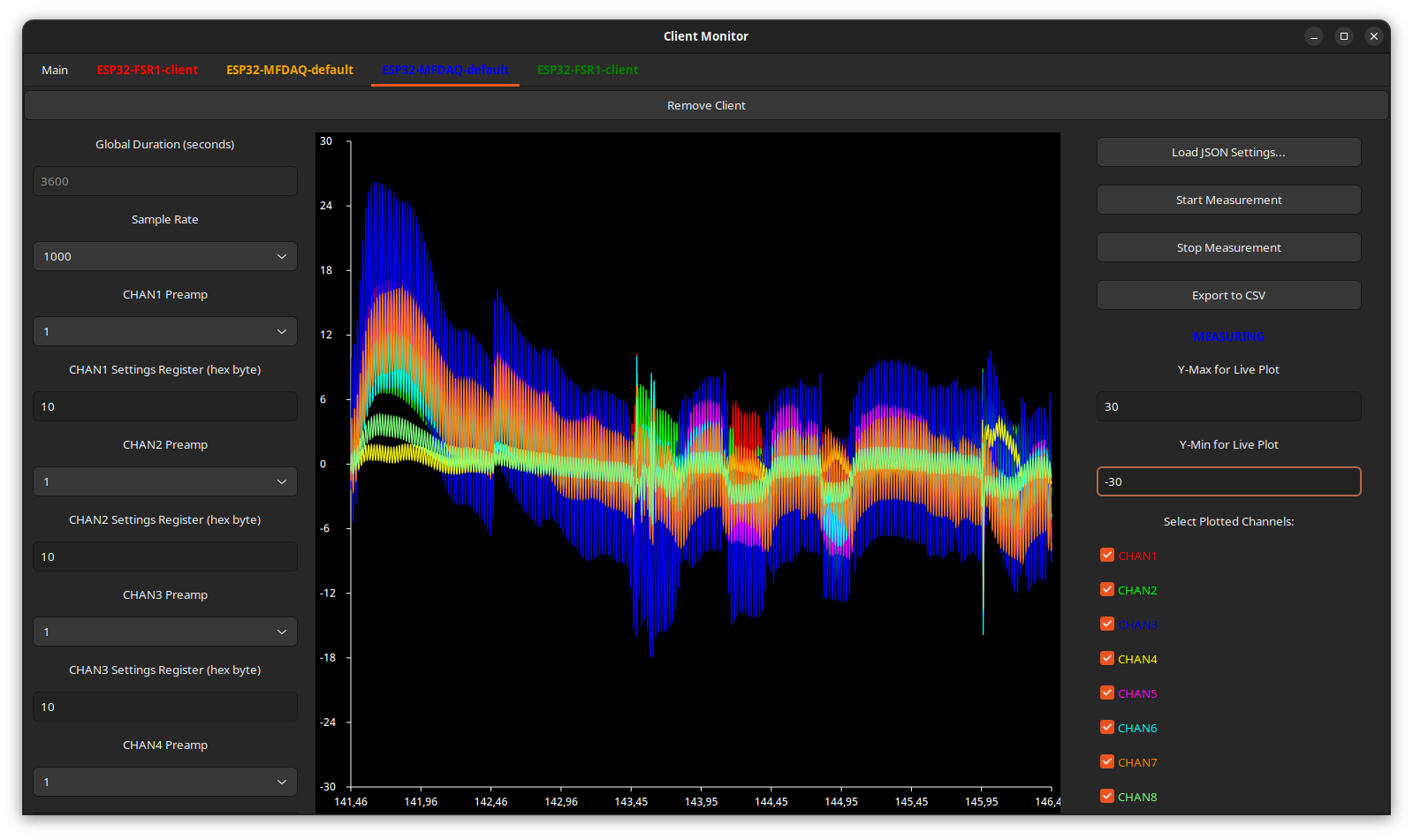
The DAQ can also be used as a client for the MMM (MultiMeasurementMonitor) project with this firmware.
The available settings stay the same, but you get the benefits of the MMM. The ClientName is set via the JSON file when programming, and the Wi-Fi credentials can be changed via the Serial Monitor at startup.
For further details on using clients with the MMM, see the MMM project on GitHub.
| Content | License |
|---|---|
| Hardware (PCB design and production files) | CERN-OHL-W-2.0 |
| Software (firmware, scripts) | MIT |
| Documentation and images | CC BY 4.0 |
Copyright (c) 2024–2026 Measurement and Sensor Technology Group (MUST), TU Darmstadt and contributors. See LICENSE for details and THIRD_PARTY_NOTICES.md for third-party components.
If you use Multi-Ferro-DAQ in your research, please cite it using the metadata in CITATION.cff (GitHub: "Cite this repository").
Developed at the Measurement and Sensor Technology Group (MUST), Technische Universität Darmstadt.
| Qty | Value | Footprint | References |
|---|---|---|---|
| 20 | TestPoint | TestPoint:TestPoint_Pad_D1.0mm | ADC_Daisy1, ADC_TESTN1, ADC_TESTP1, TP_3.3V2, TP_5V1, TP_ADC_*PWDN1, TP_ADC_*RST1, TP_CS1, TP_DRDY1, TP_GND1, TP_GND2, TP_MISO1, TP_MOSI1, TP_OP_N1, TP_OP_OUT1, TP_OP_P1 +4 |
| 16 | 10u | Capacitor_SMD:C_0603_1608Metric | C1, C8, C9, CS2, CS9, CS11, CS16, CS18, CS31, CS34, CS39, CS40, CS41, CS42, CS50, CS52 |
| 14 | 100n | Capacitor_SMD:C_0603_1608Metric | CS1, CS3, CS15, CS17, CS19, CS29, CS32, CS37, CS38, CS43, CS44, CS46, CS51, CS53 |
| 11 | 1u | Capacitor_SMD:C_0603_1608Metric | CCH1, CS4, CS5, CS7, CS8, CS10, CS12, CS13, CS14, CS47, CS48 |
| 8 | 1G | Resistor_SMD:R_0805_2012Metric_Pad1.20x1.40mm_HandSolder | RF1, RF2, RF3, RF4, RF5, RF6, RF7, RF8 |
| 8 | 680p | Capacitor_SMD:C_0805_2012Metric_Pad1.18x1.45mm_HandSolder | CF1, CF2, CF3, CF4, CF5, CF6, CF7, CF8 |
| 7 | 10k | Resistor_SMD:R_0603_1608Metric | R1, R2, R12, R13, R15, R16, R17 |
| 4 | 0R | Resistor_SMD:R_0603_1608Metric | R28, R29, R30, Rf_Op1 |
| 3 | 100R | Resistor_SMD:R_0603_1608Metric | R3, R4, R5 |
| 3 | 22u | Capacitor_SMD:C_0603_1608Metric | CS6, CS28, CS30 |
| 3 | LOGO | LOGO | G***, G***, G*** |
| 2 | 10n | Capacitor_SMD:C_0603_1608Metric | CS33, CS49 |
| 2 | 3.57k | Resistor_SMD:R_0603_1608Metric | R7, R33 |
| 2 | 5.1k | Resistor_SMD:R_0603_1608Metric | R19, R20 |
| 2 | 8P8C_Shielded | R-RJ45R08P-B000:R-RJ45R08P-B000 | J1, J5 |
| 2 | AD8608ARUZ-REEL | AD8608ARUZ:RU_14_ADI | U1, U4 |
| 2 | Conn_01x02_Pin | Connector_PinHeader_2.54mm:PinHeader_1x02_P2.54mm_Vertical | GPIO1, GPIO2 |
| 2 | Conn_01x04_Socket | Connector_JST:JST_SH_BM04B-SRSS-TB_1x04-1MP_P1.00mm_Vertical | J2, J3 |
| 2 | FerriteBead | Inductor_SMD:L_0603_1608Metric | FB1, FB2 |
| 2 | LED_R | LED_SMD:LED_0603_1608Metric | D2, D3 |
| 2 | SK6812MINI-HS | SK6812MNI-HS:SK6812MNI-HS | D5, D6 |
| 2 | SKRPABE010 | SKRPABE010:SW_SKRPABE010 | S2, S3 |
| 2 | SolderJumper_2_Bridged | Jumper:SolderJumper-2_P1.3mm_Bridged2Bar_RoundedPad1.0x1.5mm | JP_SH/GND1, JP_SH/USB1 |
| 2 | SolderJumper_3_Bridged12 | Jumper:SolderJumper-3_P1.3mm_Bridged2Bar12_RoundedPad1.0x1.5mm | JP1, JP4 |
| 1 | 1.15k | Resistor_SMD:R_0603_1608Metric | R32 |
| 1 | 1k | Resistor_SMD:R_0603_1608Metric | R6 |
| 1 | 27R | Resistor_SMD:R_0603_1608Metric | R27 |
| 1 | 680n | Capacitor_SMD:C_0603_1608Metric | CS21 |
| 1 | ADS131E08IPAGR | ADS131E08IPAGR:QFP50P1200X1200X120-64N | IC1 |
| 1 | Choke_Wurth_WE-CNSW_744232090 | Inductor_SMD:L_CommonMode_Wurth_WE-CNSW-1206 | L1 |
| 1 | Conn_01x02_Pin | Connector_PinHeader_1.27mm:PinHeader_1x02_P1.27mm_Vertical | UART0 |
| 1 | Conn_01x02_Pin | Connector_JST:JST_PH_B2B-PH-K_1x02_P2.00mm_Vertical | J4 |
| 1 | DMG2305 | DMG2305UX:DMG2305UX | Q1 |
| 1 | D_Schottky | Diode_SMD:D_SOD-323 | D1 |
| 1 | ESP32-S3-MINI-1-N8 | ESP32-S3-MINI-1-N8:XCVR_ESP32-S3-MINI-1-N8 | U2 |
| 1 | ICM-42670-P | ICM-42670-P:LGA14_2.5X3X0.76_IVS | U3 |
| 1 | JP_Pullup_MOSI/SDA | Jumper:SolderJumper-2_P1.3mm_Open_RoundedPad1.0x1.5mm | JP3 |
| 1 | JP_Pullup_SCL/SCLK | Jumper:SolderJumper-2_P1.3mm_Open_RoundedPad1.0x1.5mm | JP2 |
| 1 | LED_W | LED_SMD:LED_0603_1608Metric | D4 |
| 1 | LM2775QDSGRQ1 | LM2775QDSGRQ1:SON50P200X200X80-9N | IC7 |
| 1 | MountingHole_Pad | MountingHole:MountingHole_3.2mm_M3_Pad | H2 |
| 1 | RFShield_TwoPieces | RF_Shielding:Laird_Technologies_BMI-S-204-F_32.00x32.00mm | J7 |
| 1 | SK-12D02-VG3 | SK-12D02-VG3:SK12D02VG3 | S1 |
| 1 | SolderJumper_2_Open | Jumper:SolderJumper-2_P1.3mm_Open_RoundedPad1.0x1.5mm | JP_ADC_RefP1 |
| 1 | TLV9051IDBVR | TLV9051IDBVR:SOT95P280X145-5N | IC3 |
| 1 | TP4056 | TP4056:SOP127P600X175-9N | IC2 |
| 1 | TPS7A9101DSKR | TPS7A9101DSKR:SON50P250X250X80-11N-D | IC5 |
| 1 | TYPE-C-31-M-12 | TYPE-C-31-M-12:HRO_TYPE-C-31-M-12 | J6 |
| 1 | TestPoint | TestPoint:TestPoint_THTPad_D1.0mm_Drill0.5mm | CS_External1 |
| 1 | WE-TVS-82400102 | Package_TO_SOT_SMD:SOT-23-6 | U5 |
It measures 50 × 65 mm and has 4 copper layers, 1.56 mm thick.
149 parts, built around the ESP32-S3-MINI-1-N8, ADS131E08IPAGR, LM2775QDSGRQ1 and AD8608ARUZ-REEL. The full list of its parts is on this page, with links to each part's symbol and footprint where PCBKit's library has them.
From the TUDA-MUST/Multi-Ferro-DAQ repository on GitHub, at the commit this page was made from: the board is PCB/Multi-Ferro-DAQ.kicad_pcb and its schematic PCB/ADC.kicad_sch. PCBKit opens the board in the browser, with nothing to install.
Its repository states no licence, so its author keeps all rights: ask TUDA-MUST before reusing the design.

embeddedos-org/eCAD-Hardware-Products
Hardware designs + EE docs + Board datasheets of Multiple products

lewipewi/harpy-board
Hard real-time sequencer and power hub for a Canopy Hunter hopping robot (coming soon!). Drives four servos and one brushed motor, holds attitude across a 512 ms ballistic arc, charges the cell, and logs every hop to…

daleondev/ProtoMate_Control
Open ProtoMate.kicadpro in KiCad 10. The complete system schematic and linked perfboard layout share the same project name and component identities.


FBIopeningUPP/MateRix
MateRix a esp32 s3 and ws2812b 2020 40x40 matrix display with joystick and imu and some buttons for fun


monash-human-power/power-meter
Power meter designed as part of Oscar Varney and Jotham Gates' FYP in 2024