4 layers24.5 × 14 mm

 tombueng/emcvisual3
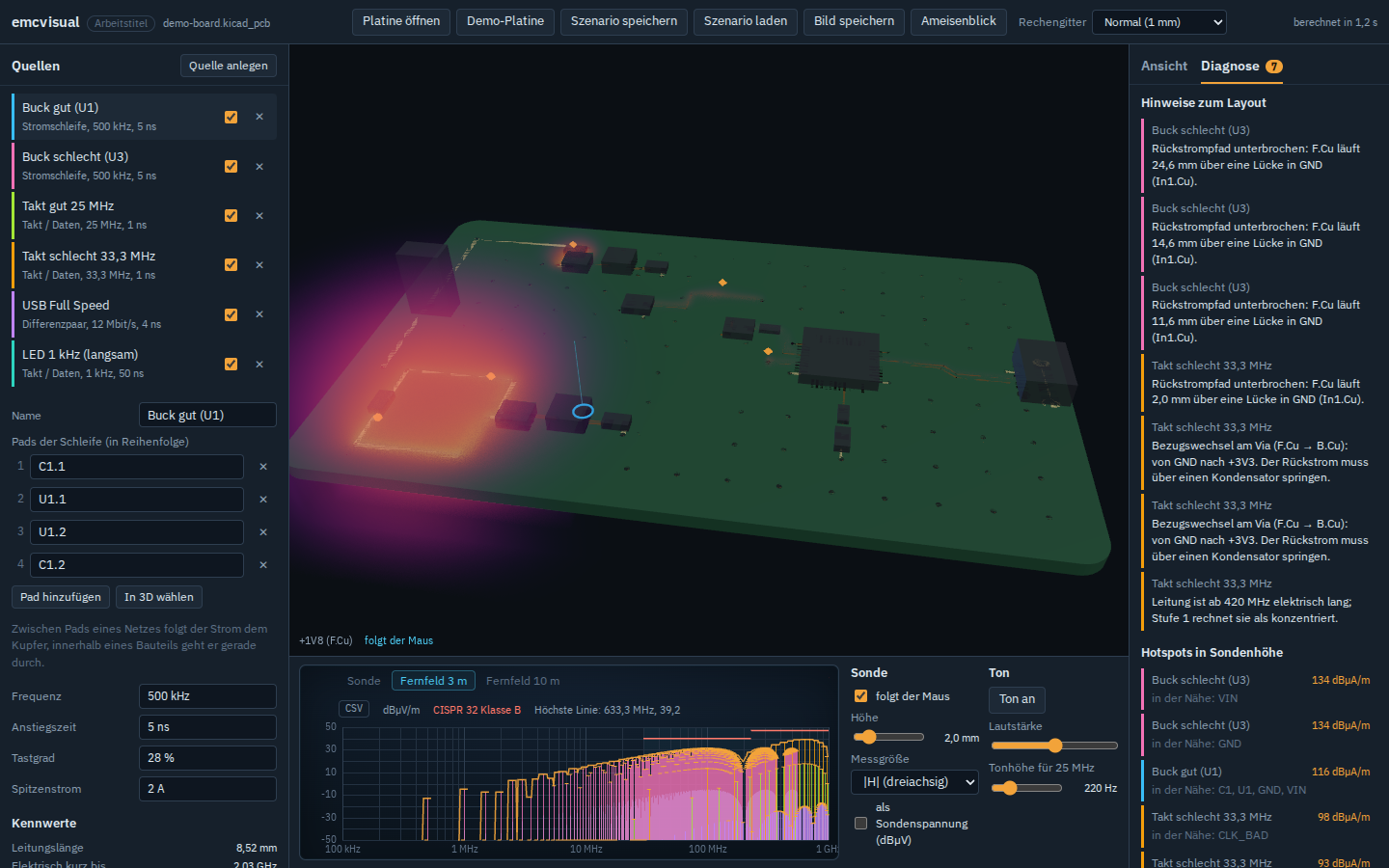
EMC/EMI near-field simulator for KiCad PCBs in the browser: 3D field view, virtual near-field probe, spectrum, CISPR 32 estimate, return-path hints. EMV-Simulation für Leiterplatten.
Demo board is an open-source printed circuit board by tombueng, from the tombueng/emcvisual repository on GitHub, published under the 0BSD licence. It is a 4-layer board of 80 × 50 mm with 16 parts on 14 nets, routed with 59 tracks and 94 vias.
Its parts include 4 capacitors, 3 ICs, 2 resistors, 2 connectors and 2 inductors. It belongs with the sensors and measurement boards of this library.
Working title. The name lives only in
branding.config.jsonand can be changed with a script, see docs/RENAMING.md.
Try it in the browser: https://tombueng.github.io/emcvisual/
You cannot see the electromagnetic fields of a circuit board. This tool computes them from a board file and turns them into a 3D world you can look at and listen to: where does it glow, where does it hum, and what happens when the edge gets slower or the input capacitor moves closer to the switching regulator?
It also checks about 30 known EMC layout mistakes, says what to do first, explains every finding with its calculation and fix, and each time says why the statement could be wrong here. It is built on a catalogue of mistakes with sources (docs/research/EMC-MISTAKES-CATALOGUE.md), a technical review (docs/review/TECHNICAL-REVIEW-2026-10.md), generated boards with each mistake as a test bench, and a comparison with a full-wave simulation.
Everything runs in the browser. The board file does not leave your computer. The user interface speaks English and German.
| Format | From |
|---|---|
KiCad .kicad_pcb (6 to 10) | KiCad |
IPC-2581 .xml | Altium Designer, Cadence Allegro/OrCAD, Siemens PADS/Xpedition, Zuken, KiCad |
ODB++ archive .tgz / .zip | the same tools and most CAM software |
Eagle .brd (XML, Eagle 6 and later) | Autodesk Eagle, Fusion 360 Electronics |
| native files of Altium, Allegro, EasyEDA, CADSTAR, PADS, P-CAD, … | through KiCad's importers (tools/convert/to_kicad.py), then as .kicad_pcb |
Boards from IPC-2581 and ODB++ exports give the same board and the same results as the KiCad original (checked on real boards). Eagle stores only the outlines of copper pours; the app pours them itself, the way Eagle does. Details, export settings and limits: docs/IMPORT.md.
Stage 1 (M0–M6), working: quasi-static simulation of the magnetic near field (Biot–Savart with image currents in the reference planes), and with it:
Plan, acceptance criteria and notes: docs/stage-1/PLAN.md.
Stage 2 (in progress): return currents detour around slots in the plane and jump through the nearest stitching via or capacitor at a layer change (the detours are shown in 3D); electric field from line and node charges; stray field of open and shielded storage inductors. Details: docs/future/STAGE-2-PLANE-CURRENTS.md.
Stage 3 (in progress): full wave with openEMS. The app exports a job,
tools/openems/run_job.py computes it locally, and the result can be loaded next to the fast
model as a second field source: volume, probe, scan and far field. In the quasi-static range both
agree to about 1 dB; on a validation board the fast far field agrees with openEMS within 1 dB
between 30 and 350 MHz. Details: tools/openems/README.md,
docs/future/STAGE-3-FULL-WAVE.md.
Field check for CI: the same calculation as a Node script. It reports near field, far-field margin and layout findings per source and fails when a pull request makes something worse. The script is at https://tombueng.github.io/emcvisual/cli/field-check.mjs, instructions in docs/CI-FIELD-CHECK.md.
Stage 4 (in progress): the "Measure" tab: a 3D printer moves a near-field probe over the board, a receiver measures a spectrum at each point, and the result appears as a slice at the measuring height and as a difference to the simulation. A virtual rig measures the simulation and shows the whole chain without hardware; the drivers for OctoPrint, G-code over USB and the tinySA are written but not yet tried on a device. Details: docs/future/STAGE-4-SCANNER.md.
What comes later (plane solver, phase and waves, hand probe, VR): docs/ROADMAP.md.
npm install
npm run dev
Then choose "Load demo board" in the browser, or drop your own board on the window
(.kicad_pcb, IPC-2581 .xml, ODB++ .tgz/.zip or Eagle .brd). In Chrome and Edge the app
follows the opened file: every save in the CAD program reloads the board, and sources and view
stay (badge "live" next to the file name). The step-by-step guide to every panel is
docs/USER-GUIDE.md.
Real part models (right, under "Real 3D part models"): a KiCad board names only the path of each
part's model, such as ${KIPRJMOD}/3d/Relay.step or
${KICAD10_3DMODEL_DIR}/Package_SO.3dshapes/SOIC-8_3.9x4.9mm_P1.27mm.step. The app looks for the
file by its name:
https://github.com/<owner>/<repo> or a subfolder
…/tree/<branch>/<path>),${KIPRJMOD}/… sits next to the
.kicad_pcb),If a model exists several times, the same library folder wins, then STEP before GLB, WRL and STL. STEP is triangulated in the browser with OpenCascade (WebAssembly, in the background), with the colours from the file. Parts without a model found are listed.
Alternatively KiCad's own export: "File → Export → glTF/GLB" (without the board body) or
kicad-cli pcb export glb --no-board-body --subst-models board.kicad_pcb, then drop the .glb
on the window as well. The parts are matched by their reference; the GLB takes precedence over the
libraries. Boards from other CAD tools carry no model references; their parts are shown as boxes.
Public boards in every format the app reads, loaded straight from GitHub (also under "Examples …" in the app, grouped by format):
| Board | Format | What is on it | Licence |
|---|---|---|---|
| Glasgow revC3 | KiCad | USB interface with FPGA, level shifters, 4 layers | 0BSD |
| HackRF One | KiCad | SDR 1 MHz to 6 GHz, USB, clocks, RF section | GPL-2.0 |
| Cynthion | KiCad | USB analyser, 6 layers, several USB PHYs | CERN-OHL-P-2.0 |
| Olimex ESP32-POE Rev M2 | KiCad | ESP32 with Ethernet (50 MHz clock) and PoE converter, split planes | Apache-2.0 |
| OtterCastAudio V2 | KiCad | audio streamer with SoC, Ethernet and USB | MIT |
| nRFMicro | KiCad | nRF52840 module for keyboards, 2 layers without a ground plane, own 3D models | Unlicense |
| I²C soil moisture sensor | KiCad | capacitive sensor with I²C, 4 layers, own 3D models | Apache-2.0 |
| Arduino Uno Rev3 | Eagle | the classic, 2 layers with ground pours | CC-BY-SA-2.5 |
| SparkFun ESP32 Thing | Eagle | ESP32 with LiPo charger, 2 layers | CC-BY-SA-4.0 |
| Adafruit ESP32-S3 TFT Feather | Eagle | ESP32-S3 with TFT and USB-C, 2 layers | CC-BY-SA-3.0 |
| Particle (Spark) Core | Eagle | STM32 with Wi-Fi, 4 layers with supply layers | CC-BY-SA-4.0 |
| BeagleBone Black | IPC-2581 | single-board computer with DDR3, 6 layers, from Cadence Allegro | CC-BY-SA-3.0 |
| IPC-2581 test case 10 | IPC-2581 | 18 layers, 576-ball BGA, negative planes | test data |
| Barreleye G2 Expander | ODB++ | PCIe expander of a POWER9 server, 10 layers, split power planes | OCPHL-P-1.0 |
| Barreleye G2 power distribution | ODB++ | 12 V and 48 V distribution, 6 layers | OCPHL-P-1.0 |
| Zaius LOM/VGA card | ODB++ | network and VGA card, 4 layers, negative ground planes | OCPHL-P-1.0 |
The boards belong to their projects and are under their licences; they are not in this repository.
Boards can also be opened by link: ?demo loads the demo, ?board=<URL> a board file (any of the
formats above) from a server that allows cross-origin reads (e.g. raw.githubusercontent.com),
optionally with &models=<URL> for a GLB.
Example: Glasgow revC3.
| Command | Purpose |
|---|---|
npm run dev | development server |
npm test | tests (physics against analytic solutions, parsers against pcbnew reference data, importers against KiCad's exports, the EMC test boards) |
npm run e2e | Playwright tests in the browser (once before: npx playwright install --only-shell chromium) |
npm run check | type check (TypeScript and Svelte) |
npm run build | static site into dist/, and the field check into dist/cli/ |
npm run field-check -- board.kicad_pcb --scenario s.json | field check without a browser, e.g. in CI; also takes IPC-2581, ODB++ and Eagle files (docs/CI-FIELD-CHECK.md) |
npm run demo-board | regenerate the demo board with KiCad (pcbnew Python) |
npm run check:codename | checks that the working title appears only where it may |
It shows where current loops create magnetic fields and how changes to loop area, return path
and edges affect those fields, and it finds the known layout mistakes (checked on generated boards
with each mistake, tools/emc-cases). It does not predict whether a device passes an EMC
test: tests mostly fail on common-mode currents on cables, which the app estimates only roughly
for the worst case; there are no resonances and no enclosure. Every explanation says why its
number could be wrong here. Assumptions and limits are in
docs/stage-1/PHYSICS.md, the known kinds of mistakes in
docs/research/EMC-MISTAKES-CATALOGUE.md, the
technical review in docs/review/TECHNICAL-REVIEW-2026-10.md.
0BSD (Zero-Clause BSD): anyone may use, change and share the code for any purpose,
also commercially, without attribution. openEMS (stage 3) is under GPL-3.0 and installed
separately; it is not part of this repository. To read STEP models the app loads
occt-import-js (OpenCascade as WebAssembly,
LGPL-2.1) unchanged as its own worker with its own .wasm file; its licence applies to it.
| Qty | Value | Footprint | References |
|---|---|---|---|
| 2 | 10u | C_0805_2012Metric | C1, C3 |
| 2 | 22u | C_0805_2012Metric | C2, C4 |
| 2 | 4u7 | L_Vishay_IFSC-1515AH_4x4x1.8mm | L1, L3 |
| 2 | Buck 500 kHz (Demo) | SOT-23-6 | U1, U3 |
| 1 | 1k | R_0603_1608Metric | R3 |
| 1 | 25 MHz | Oscillator_SMD_Abracon_ASE-4Pin_3.2x2.5mm | Y1 |
| 1 | 33 | R_0603_1608Metric | R1 |
| 1 | 33.333 MHz | Oscillator_SMD_Abracon_ASE-4Pin_3.2x2.5mm | Y2 |
| 1 | LED | LED_0805_2012Metric | D1 |
| 1 | MCU (Demo) | LQFP-48_7x7mm_P0.5mm | U2 |
| 1 | USB | USB_Micro-B_Molex-105017-0001 | J2 |
| 1 | VIN 12V | PinHeader_1x02_P2.54mm_Vertical | J1 |
It measures 80 × 50 mm and has 4 copper layers, 1.6 mm thick.
16 parts. The full list of its parts is on this page, with links to each part's symbol and footprint where PCBKit's library has them.
From the tombueng/emcvisual repository on GitHub, at the commit this page was made from: the board is public/demo/demo-board.kicad_pcb. PCBKit opens the board in the browser, with nothing to install.
Its repository publishes it under the 0BSD licence: you may reuse it on that licence's terms (keep the author's notice, and for a copyleft licence share your changes alike).


mackieks/melonHD
Lontium LT6711A HDMI to USB-C DP Alt Mode Converter Module for portablizers

