4 layers54.4 × 20.3 mm

 tomasr8/attiny85-dev-board16
Fully open-source attiny85 development board
Attiny85 is an open-source printed circuit board by tomasr8, from the tomasr8/attiny85-dev-board repository on GitHub, published under the MIT licence. It is a 2-layer board of 44.6 × 16.6 mm with 14 parts on 13 nets, routed with 102 tracks and 0 vias.
It is built around the ATTINY85-20PU and AMS1117-3.3. Its parts include 5 resistors, 4 diodes, 2 ICs and 2 connectors. It belongs with the microcontroller boards boards and the AVR (ATmega, ATtiny) boards of this library.


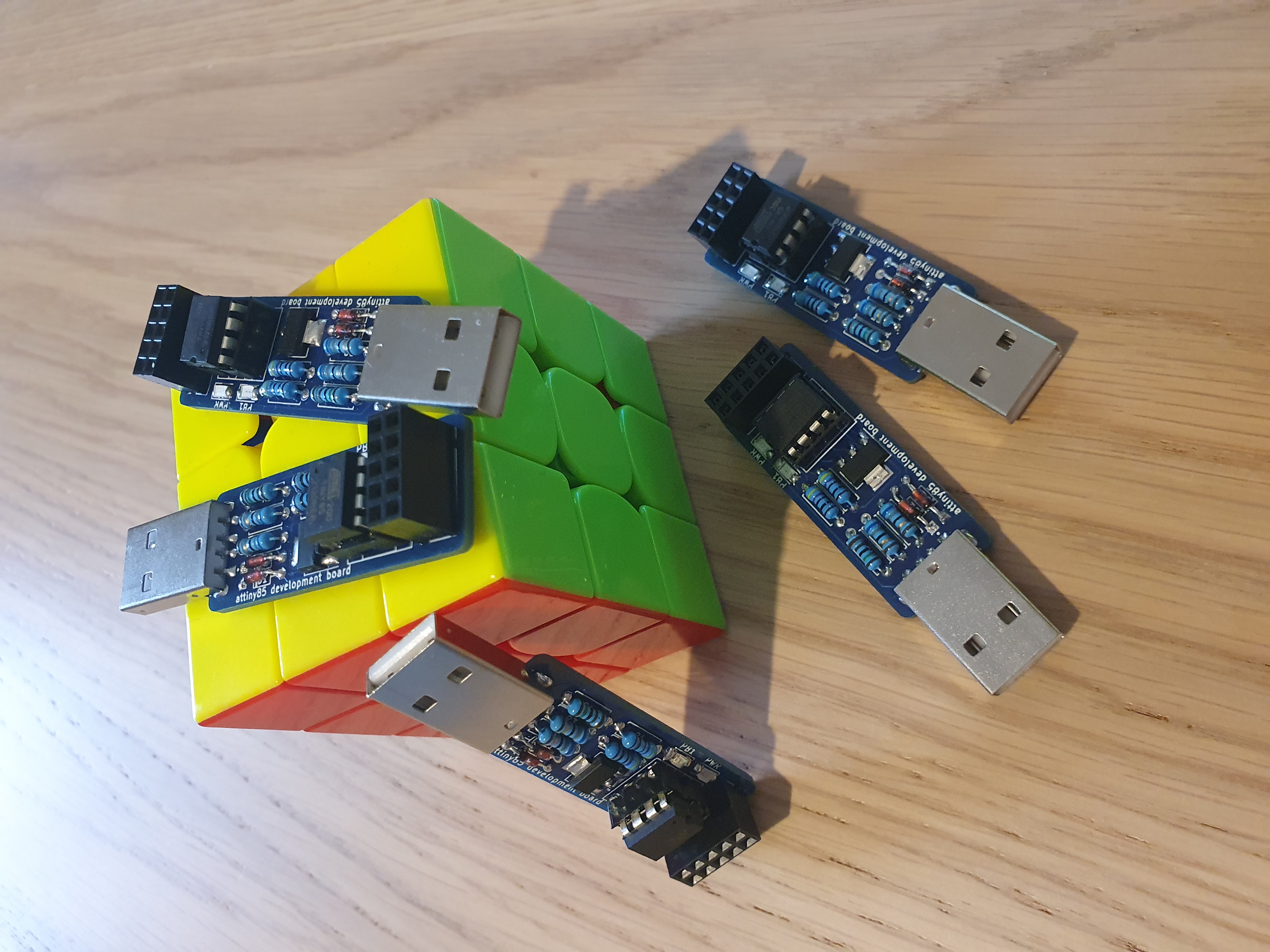
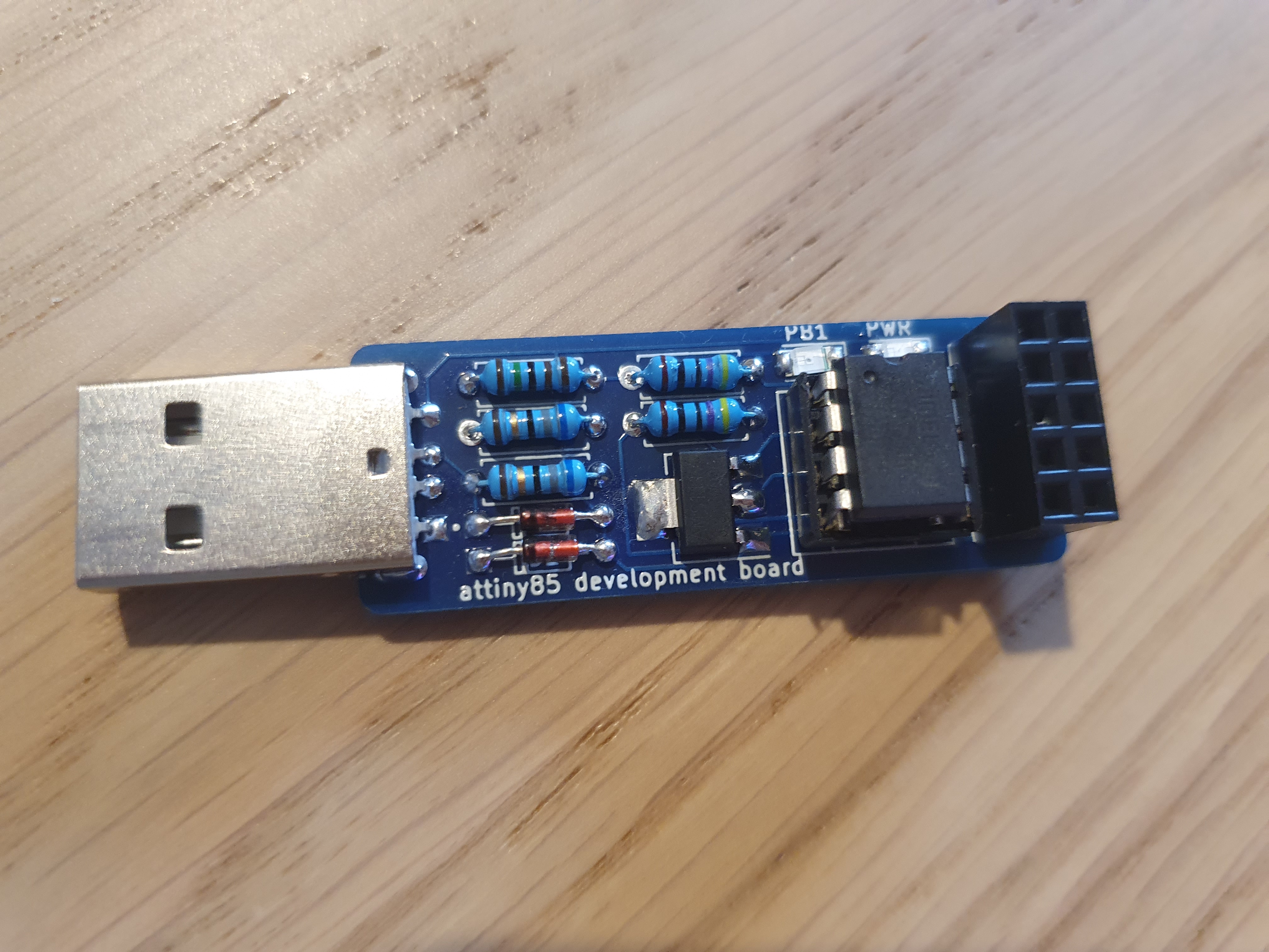
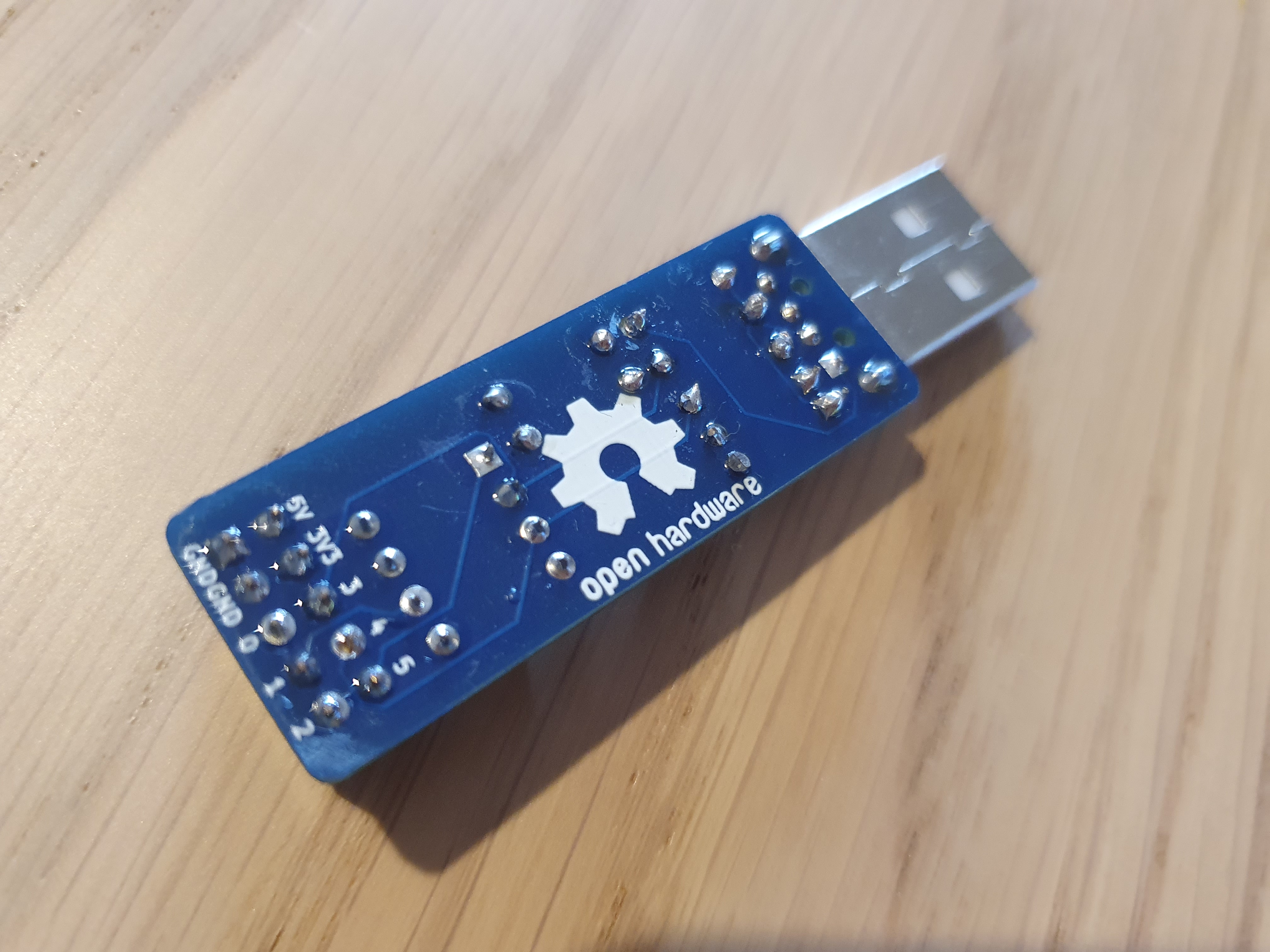
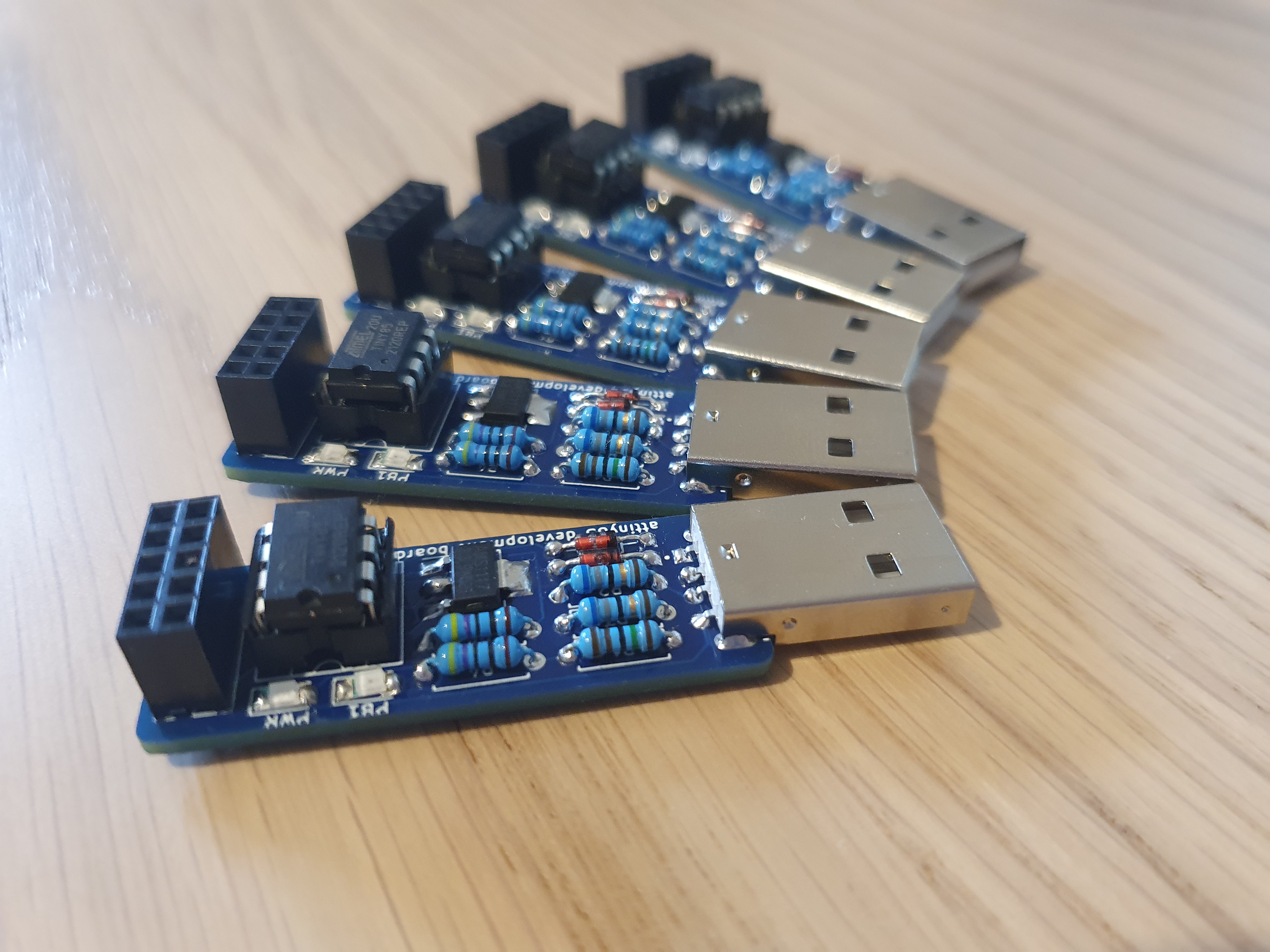
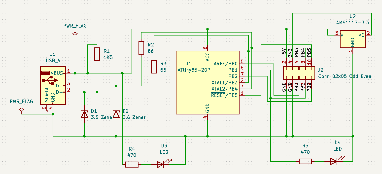
The schematic is based on the Digispark attiny85 devboard.
To learn more about electronics and PCB design and also because the Digispark boards don't have a 3V3 output. This board also uses USB-A instead of Micro USB so I don't need any extra cable to connect to my laptop.
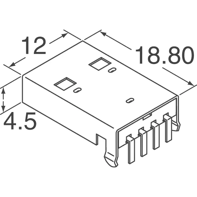
I use a custom footprint for the USB connector. You'll need to add it to your Kicad footprint library. It's a standard USB-A male connector with through hole connections for easier soldering (exact type is MOLEX 48037-0001, available on aliexpress).
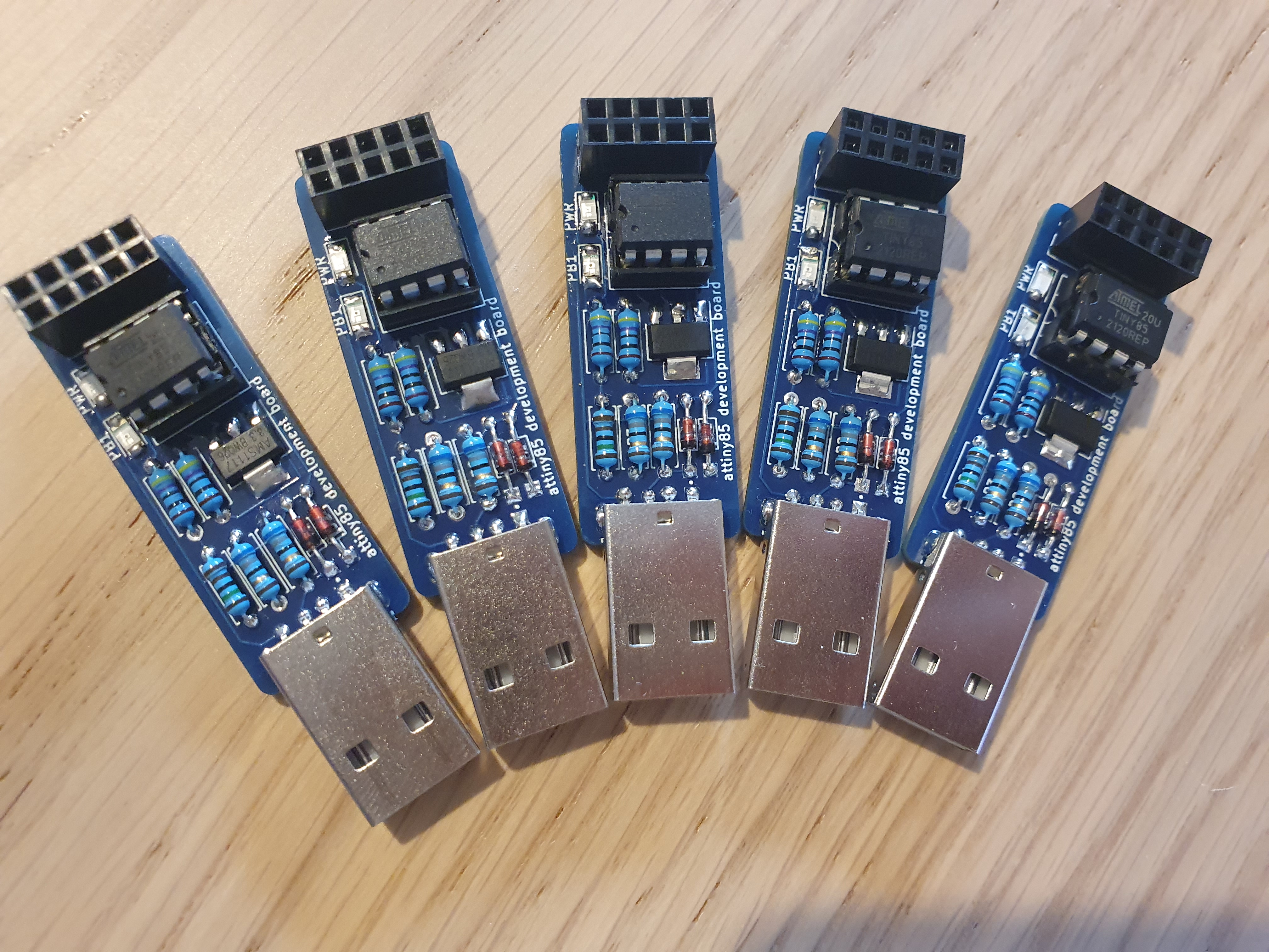
All of these components can be easily sourced from aliexpress.
I'm not great at soldering SMD components so I recommend starting with those. That would be the LEDs and the voltage regulator. After that you can continue with the chip socket and the pin header. You can finish off with the resistors/diodes and the USB connector.
The attiny chip needs to be flashed with a bootloader so that you can use it without a programmer (like an Arduino board). Here are two tutorials that I used to get mine working (you're gonna need an Arduino board to burn the bootloader):
These tutorials use the micronucleus bootloader used by the Digispark attiny boards.
There is an onboard LED hardwired to PB1 so you can get your blink sketch running without any extra hardware ;)
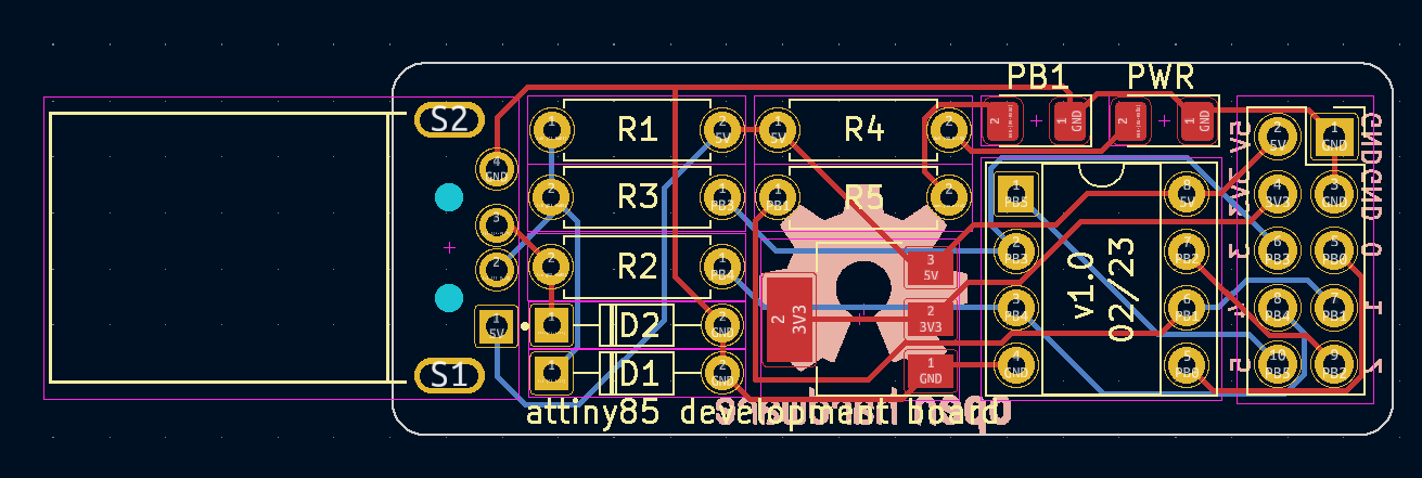
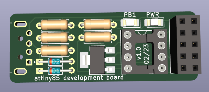
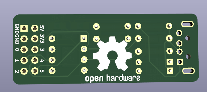
| Qty | Value | Footprint | References |
|---|---|---|---|
| 2 | 3.6 Zener | Diode_THT:D_DO-34_SOD68_P7.62mm_Horizontal | D1, D2 |
| 2 | 470 | Resistor_THT:R_Axial_DIN0207_L6.3mm_D2.5mm_P7.62mm_Horizontal | R4, R5 |
| 2 | 66 | Resistor_THT:R_Axial_DIN0207_L6.3mm_D2.5mm_P7.62mm_Horizontal | R2, R3 |
| 2 | LED | LED_SMD:LED_1206_3216Metric_Pad1.42x1.75mm_HandSolder | D3, D4 |
| 1 | 1K5 | Resistor_THT:R_Axial_DIN0207_L6.3mm_D2.5mm_P7.62mm_Horizontal | R1 |
| 1 | AMS1117-3.3 | Package_TO_SOT_SMD:SOT-223-3_TabPin2 | U2 |
| 1 | ATtiny85-20P | Package_DIP:DIP-8_W7.62mm_Socket | U1 |
| 1 | Conn_02x05_Odd_Even | Connector_PinSocket_2.54mm:PinSocket_2x05_P2.54mm_Vertical | J2 |
| 1 | USB_A | My footprints:MOLEX_48037-0001 | J1 |
The 13 most common of 14 parts.
It measures 44.6 × 16.6 mm and has 2 copper layers, 1.6 mm thick.
14 parts, built around the ATTINY85-20PU and AMS1117-3.3. The full list of its parts is on this page, with links to each part's symbol and footprint where PCBKit's library has them.
From the tomasr8/attiny85-dev-board repository on GitHub, at the commit this page was made from: the board is attiny85.kicad_pcb and its schematic attiny85.kicad_sch. PCBKit opens the board in the browser, with nothing to install.
Its repository publishes it under the MIT licence: you may reuse it on that licence's terms (keep the author's notice, and for a copyleft licence share your changes alike).

FarahCelebi/PCB-Design-Projects
A collection of PCB designs progressing from basic passive circuits to a complete USB-powered IoT sensor board — built in KiCad, covering schematic design, multi-layer layouts, power regulation, I2C communication, and…


bwack/C64-Switchless-Multi-Kernal-27C256-adapter
Kernal switcher for the C64/C64C/C128

plusvic/simplebus2-intercom
General description of the Simplebus2 protocol used by some Comelit's intercoms. Hardware for retransmitting Simplebus2 messages over UART.

osmocom/osmocom-analog
Software Implementation of analog cellular telephony systems like NMT, TACS, IMTS, A/B/C-Netz; mirror of https://gitea.osmocom.org/cellular-infrastructure/osmocom-analog

strickyak/jerboa-attiny85-mod-synth
Modular Synthesizer using an ATtiny85 chip for each module.
