Skip to the content
PCBKitNew board
2 layers59.5 × 68 mmSchema, the printed circuit board in 3D

Scanner 3D low-cost sur Raspberry Pi : ligne laser, 2 caméras, plateau rotatif → maillage STL

Size
59.5 × 68 mm
Copper layers
2
Thickness
1.6 mm
Parts
29
Nets
22
Pads
81
Tracks, vias
85, 0
Pours
1
Routed
Yes
KiCad
KiCad 10.0 (file 20260206)
Created
4 Mar 2026
Updated
15 Oct 2026

Overview

Schema is an open-source printed circuit board by tom-berthoud, from the tom-berthoud/scanner3d-pmd repository on GitHub. It is a 2-layer board of 59.5 × 68 mm with 29 parts on 22 nets, routed with 85 tracks and 0 vias.

It is built around the LM2596S-5.0 and SI2302. Its parts include 12 connectors, 8 resistors, 4 transistors and 1 IC.

Main components

2

README

README.md

Scanner 3D — donner une forme numérique au réel
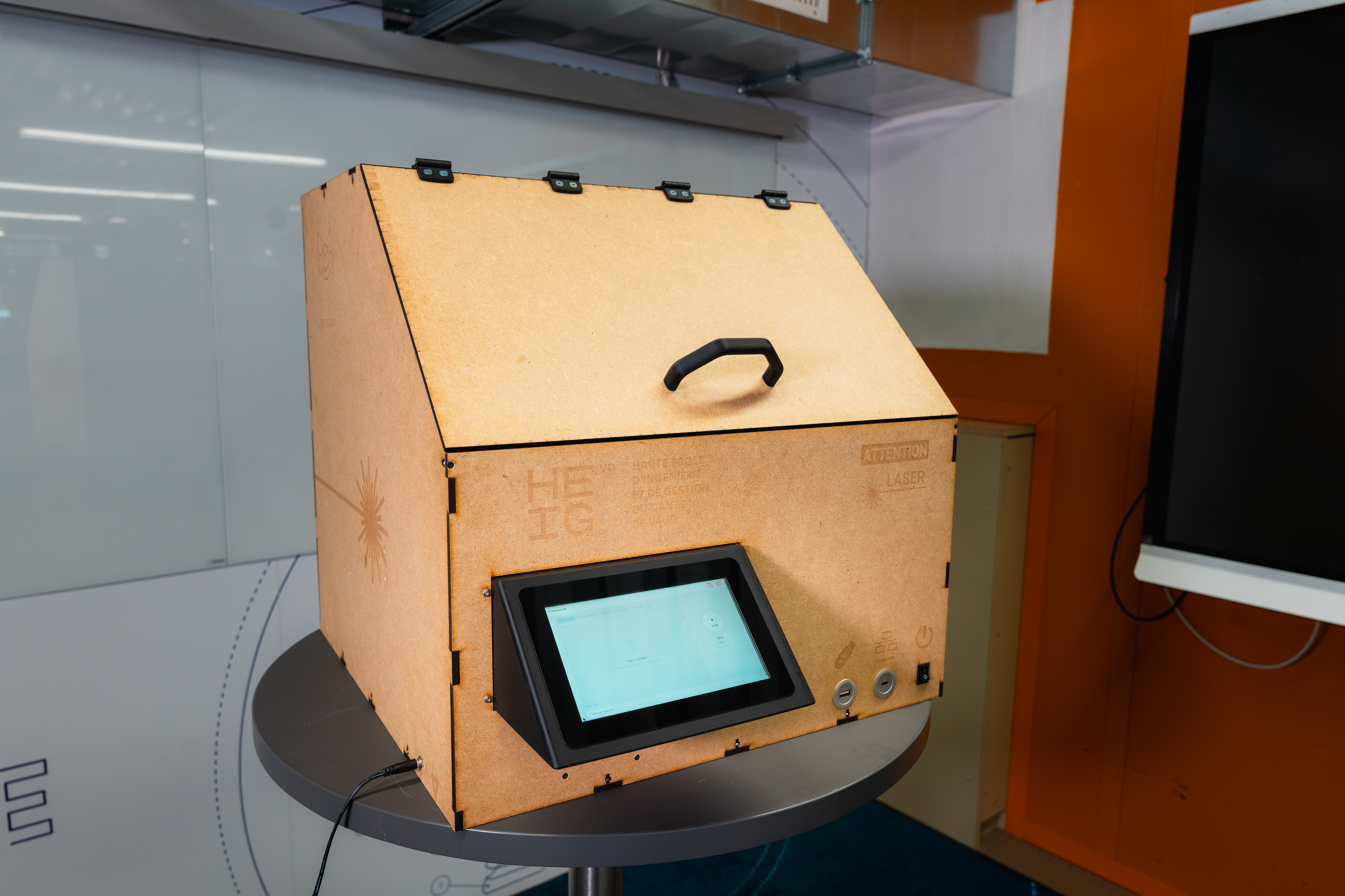
Scanner 3D fermé avec son écran tactile

Un scanner 3D open source, compact et low-cost, conçu autour d'un Raspberry Pi.
Numérisez un objet, reconstruisez sa géométrie et exportez un modèle STL prêt à être réutilisé.

Voir le poster du projet · Lire le rapport complet


Le projet en une phrase

Scanner 3D transforme un objet posé sur un plateau rotatif en un modèle numérique exploitable grâce à une ligne laser, deux caméras et une chaîne logicielle complète — de la capture au maillage STL.

De l'objet au modèle 3D
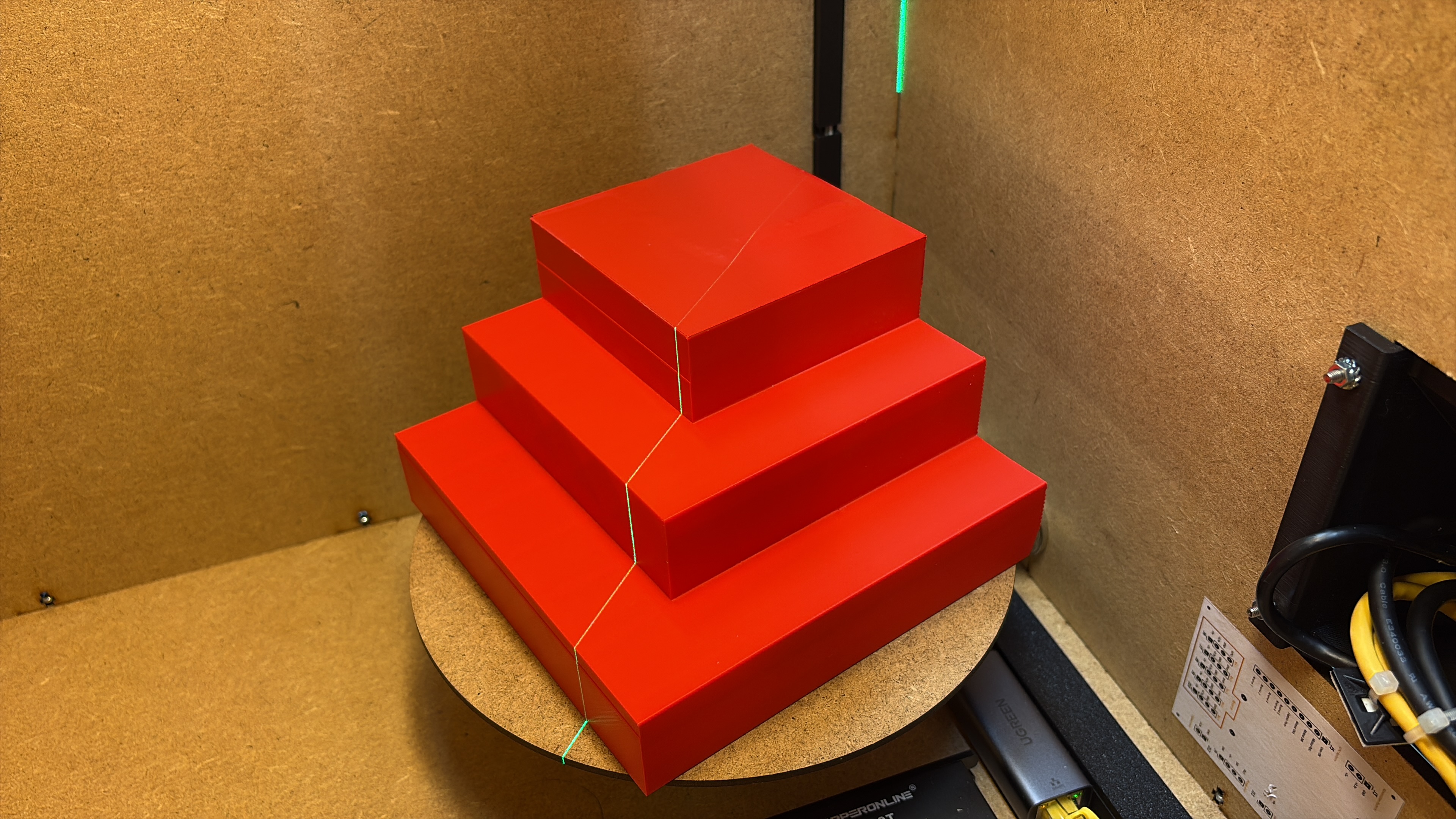
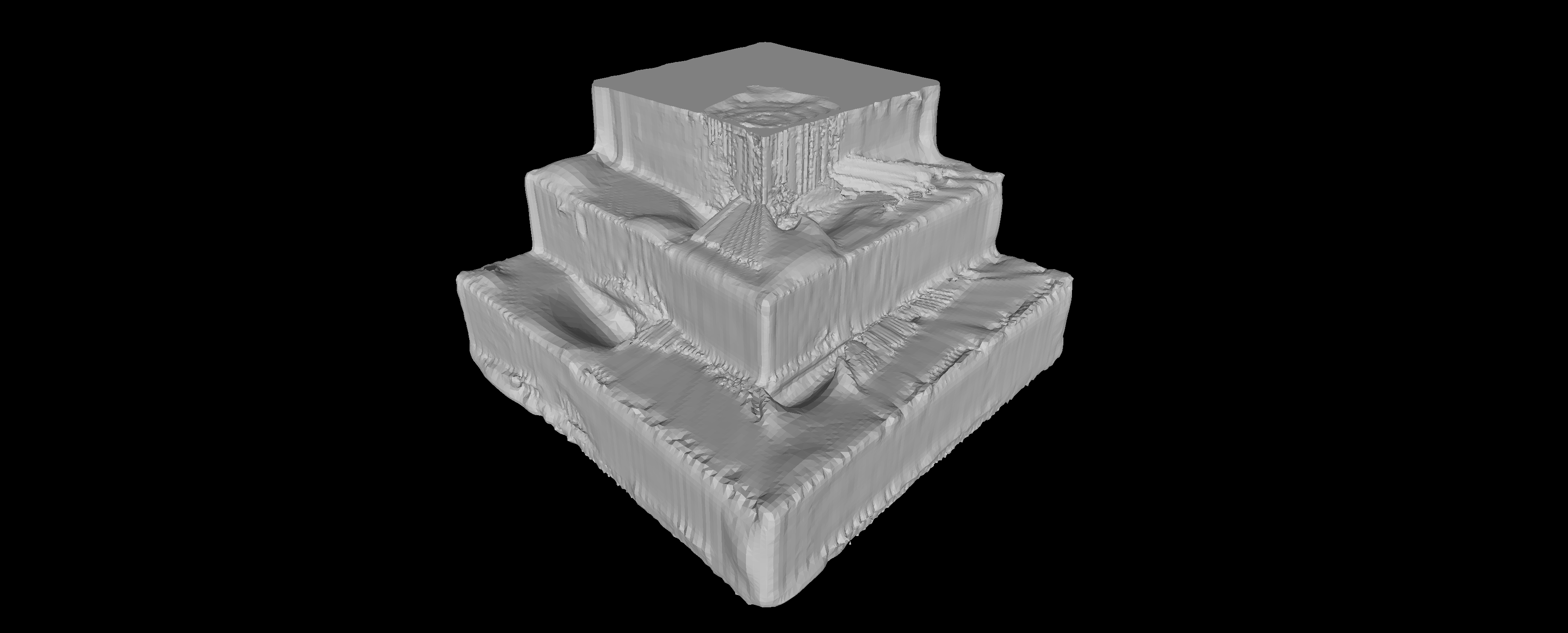
Objet éclairé par la ligne laser dans le scanner Maillage 3D reconstruit

  1. L'objet est placé au centre du plateau.
  2. Le plateau effectue une rotation progressive sur 360°.
  3. À chaque position, le laser dessine un profil lumineux et les deux caméras capturent la scène.
  4. La ligne laser est détectée puis convertie en profil 3D par triangulation.
  5. Les profils sont fusionnés en nuage de points, filtrés et transformés en maillage.
  6. Le résultat est visualisable dans l'interface et exportable en STL ou OBJ.

Pourquoi ce scanner ?

  • Accessible — une architecture low-cost pensée pour un budget d'environ 300 CHF.
  • Autonome — boîtier fermé, plateau motorisé, laser, caméras et écran tactile réunis dans un seul système.
  • Pédagogique — mécanique, électronique, vision, géométrie 3D et interface web dans un même projet.
  • Pratique — un parcours de scan simple, avec aperçu, suivi de progression et téléchargement du résultat.
  • Reproductible — configuration YAML, calibration guidée, simulation hardware et tests automatisés.

Une architecture complète
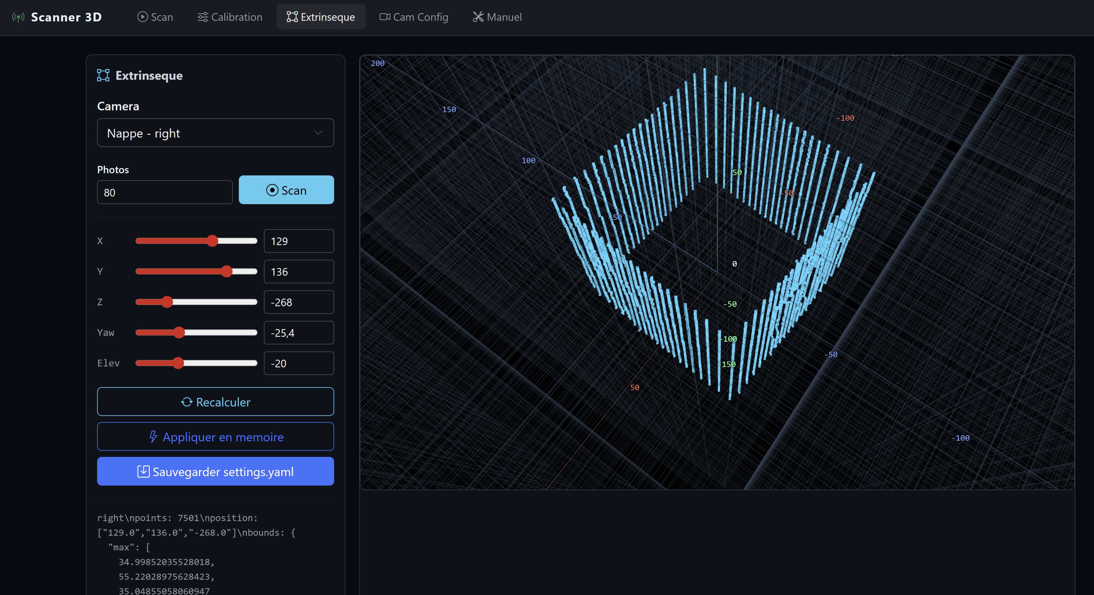
Interface web du scanner et aperçu 3D

CoucheRôle
AcquisitionCapture synchronisée des deux caméras et commande du laser
VisionDétection robuste de la ligne laser et réduction du bruit
GéométrieCalibration caméra / laser, triangulation et fusion des deux vues
ReconstructionAssemblage des profils en nuage de points puis maillage
InterfacePilotage web, aperçu caméra, progression en temps réel et viewer 3D
MatérielRaspberry Pi, moteur pas à pas, plateau rotatif, double caméra et écran local

Résultats

Le prototype répond aux objectifs du projet :

  • acquisition d'un profil 3D à chaque rotation ;
  • fusion des profils en nuage de points ;
  • génération d'un maillage STL imprimable ;
  • pilotage depuis une interface web Raspberry Pi ;
  • fonctionnement dans une boîte fermée pour maîtriser la lumière ambiante ;
  • objets ciblés jusqu'à environ 150 × 150 × 150 mm et scan visé en moins de 10 minutes.
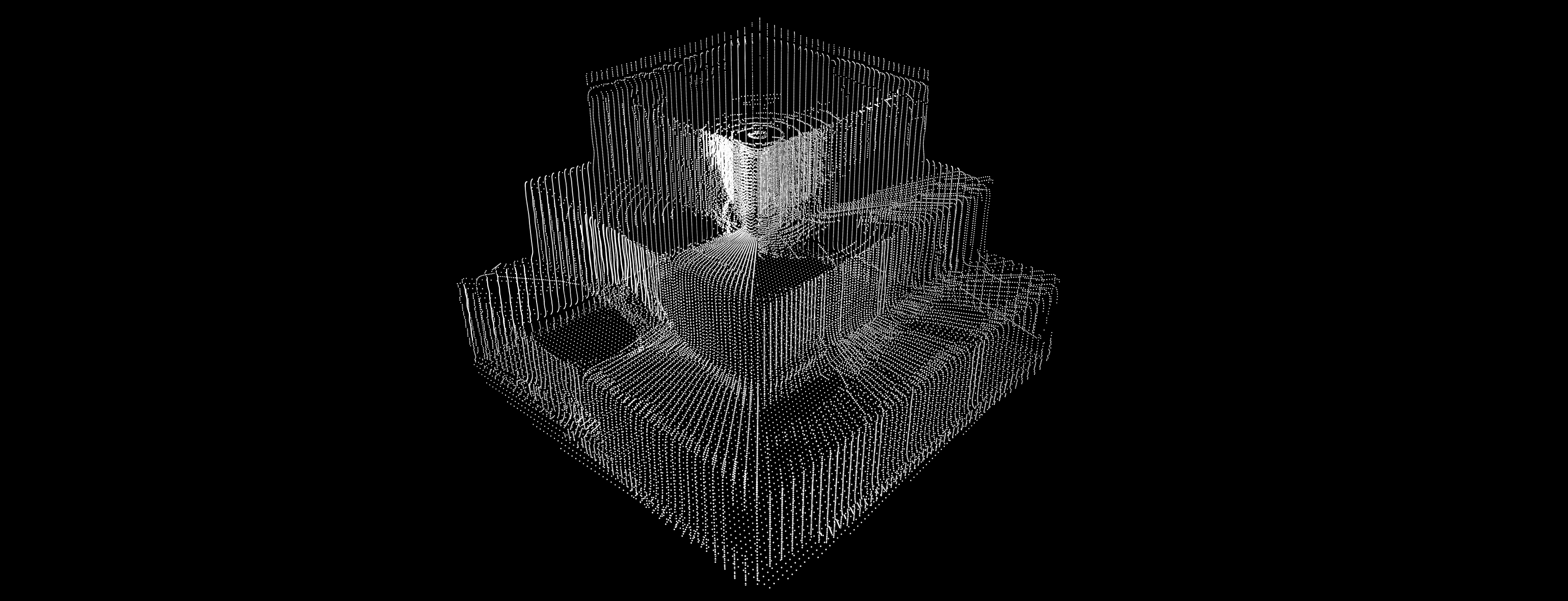
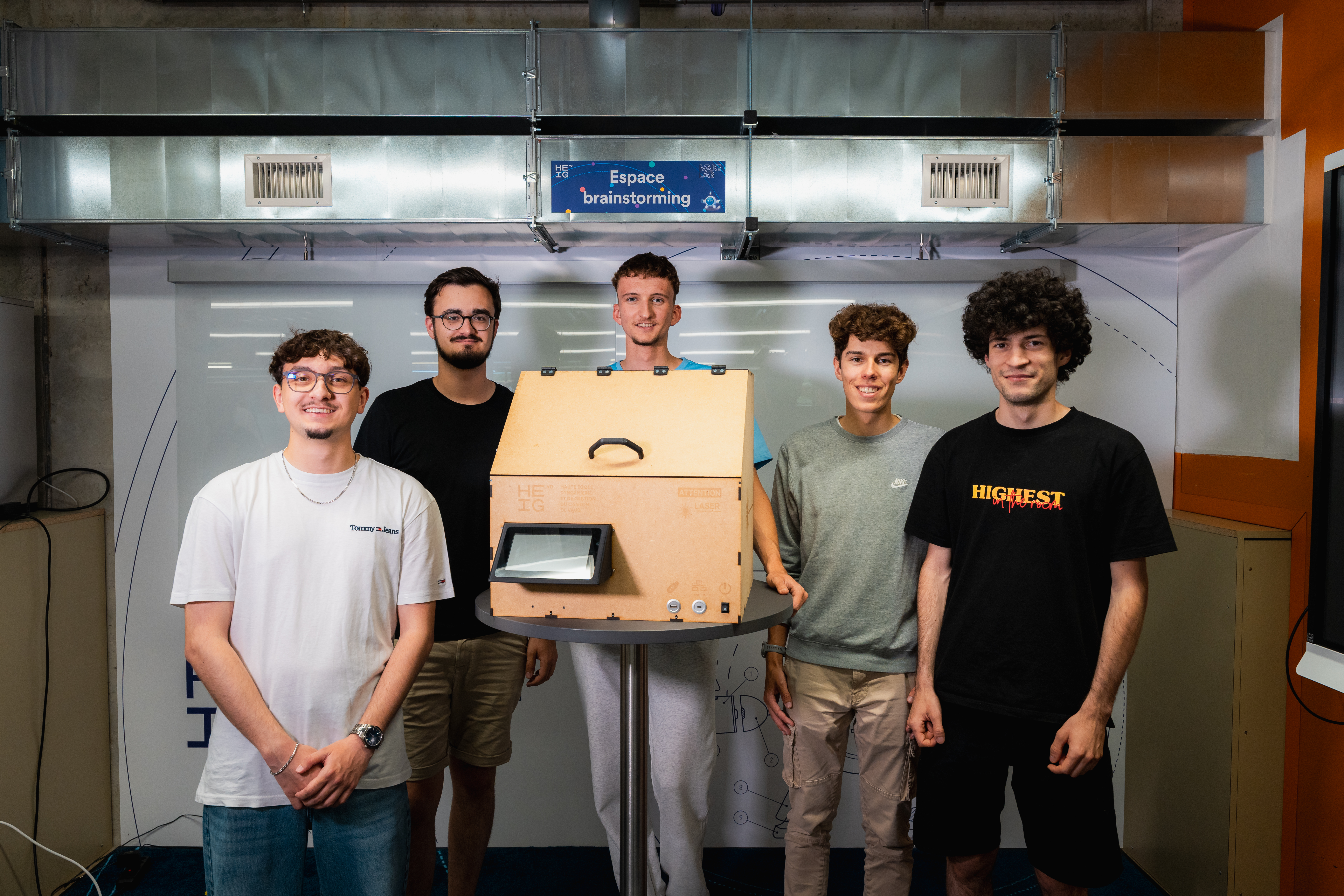
Nuage de points reconstruit Équipe présentant le prototype

Les raccourcis de déploiement, la calibration, le lancement sur Raspberry Pi et les routes de l'API sont documentés dans README-technique.md.

Explorer les ressources

L'équipe

Projet multidisciplinaire PMD — HEIG-VD, 2026

Tom Berthoud · Jason Weber · Luc Marchand · Tim Stamm · Hadrien Fuentes

Sous la responsabilité de Cédric Bornand.

Projet étudiant : le scanner est un prototype expérimental. Le laser doit rester éteint lorsque le boîtier est ouvert et ne doit jamais être regardé directement.

Parts

29
QtyValueFootprintReferences
4100Resistor_SMD:R_1206_3216MetricR5, R6, R7, R8
4100kResistor_SMD:R_1206_3216MetricR1, R2, R3, R4
4SI2302Package_TO_SOT_SMD:SOT-23Q1, Q2, Q3, Q4
1Alim RasberryConnector_PinHeader_2.54mm:PinHeader_1x03_P2.54mm_VerticalJ3
1Alim driverConnector_PinHeader_2.54mm:PinHeader_1x02_P2.54mm_VerticalJ2
1Capteur porteConnector_PinHeader_2.54mm:PinHeader_1x02_P2.54mm_VerticalJ12
1GPIO RasberryConnector_PinHeader_2.54mm:PinHeader_1x10_P2.54mm_VerticalJ5
1INConnector_PinHeader_2.54mm:PinHeader_1x02_P2.54mm_VerticalJ1
1LM2596Library_Perso:LM2596 moduleU1
1LaserConnector_PinHeader_2.54mm:PinHeader_1x02_P2.54mm_VerticalJ11
1Pilotage driverConnector_PinHeader_2.54mm:PinHeader_1x04_P2.54mm_VerticalJ4
1Res1Connector_PinHeader_2.54mm:PinHeader_1x04_P2.54mm_VerticalJ6
1Res2Connector_PinHeader_2.54mm:PinHeader_1x04_P2.54mm_VerticalJ7
1Res3Connector_PinHeader_2.54mm:PinHeader_1x04_P2.54mm_VerticalJ8
1Res4Connector_PinHeader_2.54mm:PinHeader_1x04_P2.54mm_VerticalJ9
1Res5Connector_PinHeader_2.54mm:PinHeader_1x04_P2.54mm_VerticalJ10

The 25 most common of 29 parts.

Questions

How big is the Schema PCB?

It measures 59.5 × 68 mm and has 2 copper layers, 1.6 mm thick.

What parts does the Schema use?

29 parts, built around the LM2596S-5.0 and SI2302. The full list of its parts is on this page, with links to each part's symbol and footprint where PCBKit's library has them.

Where can I download the Schema KiCad files?

From the tom-berthoud/scanner3d-pmd repository on GitHub, at the commit this page was made from: the board is docs/schema/schema.kicad_pcb and its schematic docs/schema/schema.kicad_sch. PCBKit opens the board in the browser, with nothing to install.

Can I use the Schema design in my own project?

Its repository states no licence, so its author keeps all rights: ask tom-berthoud before reusing the design.

Similar boards

  • 2 layers98.5 × 59.8 mmNeuron, the printed circuit board in 3D

    Neuron

    giant-axon/lu.i-neuron-pcb

    Lu.i is an electronic neuron circuit mimicking and illustrating the basic dynamics of real, biological neurons. The printed circuit board (PCB) features a configurable, fully analog implementation of the leaky…

    90 parts73CERN-OHL-S-2.0
  • 2 layers82 × 134 mmPcb badge, the printed circuit board in 3D

    Pcb badge

    john0312/hitcon-pcb-badge

    execute fw/merge.py to merge STM32CubeIDE generated main.c with user code in main.cc into main.cc.

    258 parts47BSD-3-Clause
  • 2 layers11 × 11 mmRtcbrd, the printed circuit board in 3D

    Rtcbrd

    adlerweb/uPoff

    Small circuit/library to shut down a µC to save power for battery powered applications

    17 parts43BSD-2-Clause
  • 2 layers307 × 85 mmCampus keyboard, the printed circuit board in 3D

    Campus keyboard

    flurples/campus

    mechanical keyboard conversion for a framework 13

    293 parts41GPL-3.0
  • 2 layers141.9 × 103.7 mmKissboard, the printed circuit board in 3D

    Kissboard

    fhtagnn/kissboard

    Hardware and Firmware for the Kissboard keyboard

    27 parts29GPL-3.0
  • 2 layers133.4 × 95.4 mmMedusa, the printed circuit board in 3D

    Medusa

    Gtrx0/Medusa

    Ble 5x7 Ortholinear Keyboard

    90 parts27
  • 2 layers133.4 × 111.4 mmAtreus split, the printed circuit board in 3D

    Atreus split

    bezmi/orthrus

    56 key wireless split keyboard running on QMK. Staggered Orthogonal layout

    34 parts26
  • 2 layers144.9 × 59.8 mmMonkeys, the printed circuit board in 3D

    Monkeys

    PacketChat/MonkeyBadge

    This repository contains the hardware design files, badge code, and backend infrastructure code for the HushCon Winter 2023 badge.

    153 parts21