4 layers28.6 × 13.9 mm

 tillitis/tk1-pcba4
PCB files for the open and flexible security key - TKey
Mta1 usb dev is an open-source printed circuit board by tillitis, from the tillitis/tk1-pcba repository on GitHub, published under the CERN-OHL-S-2.0 licence. It is a 4-layer board of 91.4 × 40.6 mm with 92 parts on 137 nets, routed with 1,192 tracks and 133 vias.
It is built around the ICE40UP5K-SG48ITR50, FT2232H MINI MODULE and W25Q80DVSNIG, with the MC2016Z48.0000C19XSH, MIC5258-1.2YM5 and USBLC6-2SC6 among its other parts. Its parts include 29 resistors, 25 capacitors, 10 ICs, 10 connectors and 5 diodes. It belongs with the FPGA and CPLD boards of this library.


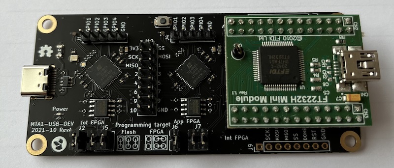
This is the original TKey design, intended as a development platform. It is a larger PCB, that connects to a PC via a USB C cable.
Main features:
2 ICE40 FPGAs.
The first ICE40 (Interface FPGA) is connected to a USB C plug, and is loaded with a gateware that contains a soft USB device. This gateware acts as an USB-to-GPIO interface to the second ICE40.
The second ICE40 (application FPGA) is loaded with a RISC-V soft core containing the security firmware. User applications are run on this gateware.
The second ICE40 also has an input button for user presenence detection.
An FTDI module is included for programming both the Application and Interface FPGAs.
Both ICE40s can be configured to boot from included SPI flash memories, NVCM, or be live programmed from the FTDI module.
All GPIO lines between the two FPGAs, as well as all programming signals, are exposed on 0.1" headers for probing.
| Qty | Value | Footprint | References |
|---|---|---|---|
| 17 | 0.10uF | mta1:CAPC1005X06L | C7, C10, C11, C12, C13, C14, C15, C16, C17, C18, C19, C20, C21, C22, C23, C24 +1 |
| 16 | 10k | mta1:ERJ2G(0402)_L | R1, R2, R8, R9, R13, R14, R15, R19, R20, R21, R22, R23, R24, R25, R26, R27 |
| 8 | 10uF | mta1:CAPC1608X09L | C1, C2, C3, C4, C5, C6, C8, C25 |
| 6 | 1K | mta1:ERJ2G(0402)_L | R4, R5, R6, R16, R17, R18 |
| 4 | MountingHole | MountingHole:MountingHole_3.2mm_M3_DIN965_Pad_TopBottom | H1, H2, H3, H4 |
| 2 | Connector_PinHeader_2.54mm:PinHeader_1x05_P2.54mm_Vertical | J1, J4 | |
| 2 | 22 | mta1:ERJ2G(0402)_L | R10, R11 |
| 2 | 5.1K | mta1:ERJ2G(0402)_L | R28, R29 |
| 2 | BLM18KG300TN1D | mta1:Ferritbead_0603_1608Metric | FB2, FB3 |
| 2 | Conn_01x08 | Connector_PinHeader_2.54mm:PinHeader_1x08_P2.54mm_Vertical | J8, J9 |
| 2 | Conn_02x01 | Connector_PinHeader_2.54mm:PinHeader_1x02_P2.54mm_Vertical | J2, J6 |
| 2 | Conn_02x02_Top_Bottom | Connector_PinHeader_2.54mm:PinHeader_2x02_P2.54mm_Vertical | J5, J7 |
| 2 | ICE40UP5K-SG48ITR | Package_DFN_QFN:QFN-48-1EP_7x7mm_P0.5mm_EP5.6x5.6mm | U3, U6 |
| 2 | LED_ARGB | mta1:0402rgb-1010 | D2, D3 |
| 2 | MBR0520 | Diode_SMD:D_SOD-123 | D4, D5 |
| 2 | W25Q80DVSNIG | Package_SO:SOIC-8_3.9x4.9mm_P1.27mm | U7, U10 |
| 1 | 100 | mta1:ERJ2G(0402)_L | R7 |
| 1 | 100mA (TBD) | Fuse:Fuse_1206_3216Metric | F1 |
| 1 | 1K5 | mta1:ERJ2G(0402)_L | R12 |
| 1 | 1V2 | TestPoint:TestPoint_Pad_D1.0mm | TP4 |
| 1 | 1k | mta1:ERJ2G(0402)_L | R3 |
| 1 | 2V5 | TestPoint:TestPoint_Pad_D1.0mm | TP3 |
| 1 | 3V3 | TestPoint:TestPoint_Pad_D1.0mm | TP2 |
| 1 | 5V | TestPoint:TestPoint_Pad_D1.0mm | TP1 |
| 1 | Conn_02x08_Odd_Even | Connector_PinHeader_2.54mm:PinHeader_2x08_P2.54mm_Vertical | J10 |
| 1 | FT2232H_MINI_MODULE | mta1:FT2232H_MINI_MODULE | U8 |
| 1 | INT_CLOCK | TestPoint:TestPoint_Pad_D1.0mm | TP5 |
| 1 | MC2016Z48.0000C19XSH | mta1:MC2016Z | U4 |
| 1 | MCP1824T-2502EOT | Package_TO_SOT_SMD:SOT-23-5 | U1 |
| 1 | MIC5258-1.2YM5 | Package_TO_SOT_SMD:SOT-23-5 | U2 |
| 1 | NCP752BSN33T1G | mta1:NCP752BSN33T1G | U9 |
| 1 | Power LED | LED_SMD:LED_0402_1005Metric | D1 |
| 1 | SW_Push | Button_Switch_SMD:SW_Push_SPST_NO_Alps_SKRK | SW1 |
| 1 | USBLC6-2SC6 | Package_TO_SOT_SMD:SOT-23-6 | U5 |
| 1 | USB_C_Receptacle_USB2.0 | Connector_USB:USB_C_Receptacle_HRO_TYPE-C-31-M-12 | J3 |
It measures 91.4 × 40.6 mm and has 4 copper layers, 1.62 mm thick.
92 parts, built around the ICE40UP5K-SG48ITR50, FT2232H MINI MODULE, W25Q80DVSNIG and MC2016Z48.0000C19XSH. The full list of its parts is on this page, with links to each part's symbol and footprint where PCBKit's library has them.
From the tillitis/tk1-pcba repository on GitHub, at the commit this page was made from: the board is prototypes/mta1-usb-dev/mta1_usb_dev.kicad_pcb and its schematic hw/application_fpga.kicad_sch. PCBKit opens the board in the browser, with nothing to install.
Its repository publishes it under the CERN-OHL-S-2.0 licence: you may reuse it on that licence's terms (keep the author's notice, and for a copyleft licence share your changes alike).

kr-Eliza/tkey-open-hardware-reproduction
Reproducing the Tillitis TKey open hardware security key: 2-layer hand-solderable PCB, lab assembly and bring-up, Voltera prototype, SBOM


riktw/HUB75E_ICE40
SpinalHDL code to drive a 64*64 pixel HUB75E module with an ICE40

matthewcieplak/super-sixteen
Code and schematics for the Super Sixteen Eurorack sequencer


oskarengdahl/Powerbank-MPD-XP
A powerbank to primarily use with MDP-XP Modular Power Supply

iank/julia_lcd
TFT LCD panel, capacitive touch controller, Xilinx Cyclone IV FPGA, SDR SDRAM