4 layers82.6 × 116.7 mm

 szfate/BondTest72
BondTest72 mainboard design files
BondTest72 is an open-source printed circuit board by szfate, from the szfate/BondTest72 repository on GitHub. It is a 4-layer board of 80 × 90 mm with 71 parts on 144 nets, routed with 1,017 tracks and 305 vias.
It is built around the ICL7660N, CH446X and SK6812. Its parts include 17 capacitors, 5 resistors, 4 ICs, 3 connectors and 2 diodes. It belongs with the RP2040 boards of this library.


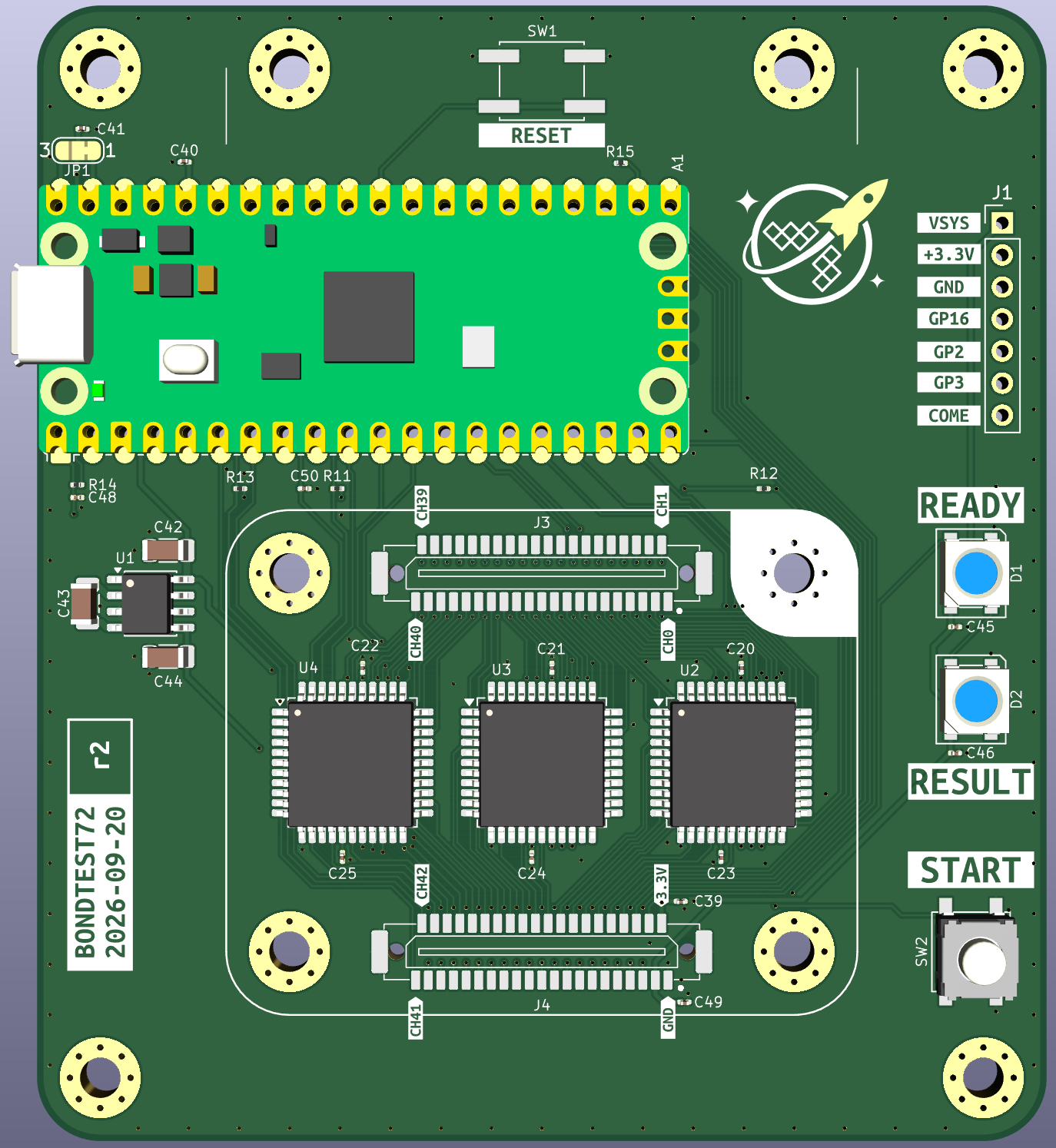
Production test fixture board for bond wire testing, controlled by a Raspberry Pi Pico. Test signals are routed through CH446X analog crosspoint switches to two 41-pin connectors, on which a replaceable adapter board sits. The adapter board carries the DUT connector and any auxiliary components, keeping the main tester board from wearing out.
| Parameter | Value |
|---|---|
| Revision | r2 |
| Date | 2026-09-20 |
| Board size | 80 × 90 mm |
| Layers | 4 (F.Cu / In1.Cu / In2.Cu / B.Cu) |
| Thickness | 1.6 mm FR4 |
The board is powered from the Pico's USB VBUS rail. The TPS7A0533 LDO provides an optional quiet +3.3VADC rail as an alternative ADC reference, in case the main +3.3V rail from the Pico's onboard DCDC is too noisy. In practice the application only requires ~0.1 V accuracy, so the main rail is likely sufficient.
An ICL7660 charge-pump voltage inverter (or equivalent) generates the negative VEE rail required by the CH446X analog crosspoint switches.
A single push button serves as the START control. The two SK6812 RGB LEDs serve as status indicators. Both the LEDs and the button sit on the right edge of the board so the prodcution panel cannot cover them.
Four CH446X analog crosspoint switches fan test signals out from the Pico GPIO/ADC lines to the 41-pin connectors (J3 / J4). These connect to a removable adapter board rather than directly to the DUT. The adapter board carries the DUT-side connector (the high-wear part) and any auxiliary components needed for a given test configuration — for example, diodes for self-testing or a small memory chip for wear-cycle monitoring. Replacing the adapter board instead of the whole fixture avoids discarding the tester after the DUT connector wears out (~100 cycles). Solder jumpers on the main board provide flexibility to work around any schematic design flaws discovered after fabrication.
Schematic:
PCB:
Initial release. 80 × 100 mm.
| File | Description |
|---|---|
BondTest72.kicad_pro | KiCad project |
BondTest72.kicad_sch | Schematic |
BondTest72.kicad_pcb | PCB layout |
docs/BondTest72-r2-schematic.pdf | r2 schematic PDF export |
docs/BondTest72-r1-schematic.pdf | r1 schematic PDF export |
production/BondTest72-r2.zip | r2 gerber/fabrication outputs |
production/BondTest72-r2-bom.csv | r2 bill of materials |
production/BondTest72-r2-pos.xlsx | r2 pick-and-place positions |
lib.kicad_sym | Project symbol library |
lib.pretty/ | Project footprint library |
df9.pretty/ | Additional footprint library |
docs/ | Board renders and documentation images |
| Qty | Value | Footprint | References |
|---|---|---|---|
| 11 | 100n | Capacitor_SMD:C_0201_0603Metric | C20, C21, C22, C23, C24, C25, C39, C45, C46, C48, C49 |
| 3 | 10u | Capacitor_SMD:C_1206_3216Metric | C42, C43, C44 |
| 3 | CH446X | Package_QFP:LQFP-44_10x10mm_P0.8mm | U2, U3, U4 |
| 3 | NetTie_2 | lib:NetTie-2_SMD_Pad0.15mm | NT1, NT2, NT3 |
| 2 | 1u | Capacitor_SMD:C_0201_0603Metric | C40, C41 |
| 2 | Conn_2Rows-41Pins_MountingPin | df9:DF9-41P-1V | J3, J4 |
| 2 | SK6812 | LED_SMD:LED_SK6812_PLCC4_5.0x5.0mm_P3.2mm | D1, D2 |
| 1 | 100k | Resistor_SMD:R_0201_0603Metric | R15 |
| 1 | 10k | Resistor_SMD:R_0201_0603Metric | R14 |
| 1 | 120pF | Capacitor_SMD:C_0201_0603Metric | C50 |
| 1 | 2.49k | Resistor_SMD:R_0201_0603Metric | R12 |
| 1 | 27.4K | Resistor_SMD:R_0201_0603Metric | R11 |
| 1 | 280k | Resistor_SMD:R_0201_0603Metric | R13 |
| 1 | Conn_01x07 | Connector_PinHeader_2.54mm:PinHeader_1x07_P2.54mm_Vertical | J1 |
| 1 | G*** | kibuzzard-6AAFDFCA | kibuzzard-6AAFDFCA |
| 1 | G*** | kibuzzard-6A01F806 | kibuzzard-6A01F806 |
| 1 | G*** | kibuzzard-6A027603 | kibuzzard-6A027603 |
| 1 | G*** | kibuzzard-6A01F81D | kibuzzard-6A01F81D |
| 1 | G*** | kibuzzard-6AAFFF2E | kibuzzard-6AAFFF2E |
| 1 | G*** | kibuzzard-6A030225 | kibuzzard-6A030225 |
| 1 | G*** | kibuzzard-6AAFDF39 | kibuzzard-6AAFDF39 |
| 1 | G*** | kibuzzard-6A01F62B | kibuzzard-6A01F62B |
| 1 | G*** | kibuzzard-6A01FB9A | kibuzzard-6A01FB9A |
| 1 | G*** | kibuzzard-6A01F8AF | kibuzzard-6A01F8AF |
| 1 | G*** | kibuzzard-6A01F618 | kibuzzard-6A01F618 |
| 1 | G*** | kibuzzard-6A01F8BD | kibuzzard-6A01F8BD |
| 1 | G*** | kibuzzard-6A02A7B4 | kibuzzard-6A02A7B4 |
| 1 | G*** | kibuzzard-6A01F87F | kibuzzard-6A01F87F |
| 1 | G*** | kibuzzard-6A01FE13 | kibuzzard-6A01FE13 |
| 1 | G*** | kibuzzard-6A01F655 | kibuzzard-6A01F655 |
| 1 | G*** | kibuzzard-6A01F644 | kibuzzard-6A01F644 |
| 1 | G*** | kibuzzard-6A01F88E | kibuzzard-6A01F88E |
| 1 | G*** | kibuzzard-6A02FF2D | kibuzzard-6A02FF2D |
| 1 | G*** | kibuzzard-6A01F65D | kibuzzard-6A01F65D |
| 1 | G*** | kibuzzard-6A02760F | kibuzzard-6A02760F |
| 1 | G*** | kibuzzard-6AAFFF26 | kibuzzard-6AAFFF26 |
| 1 | ICL7660 | Package_SO:SOIC-8_3.9x4.9mm_P1.27mm | U1 |
| 1 | RaspberryPi_Pico | Module:RaspberryPi_Pico_Common_Unspecified | A1 |
| 1 | SW_Push | Button_Switch_SMD:SW_SPST_EVQQ2 | SW1 |
| 1 | SW_Push | Button_Switch_SMD:SW_SPST_EVPBF | SW2 |
| 1 | SolderJumper_2_Bridged | Jumper:SolderJumper-2_P1.3mm_Bridged_RoundedPad1.0x1.5mm | JP4 |
| 1 | SolderJumper_3_Bridged12 | Jumper:SolderJumper-3_P1.3mm_Bridged12_RoundedPad1.0x1.5mm_NumberLabels | JP1 |
The 61 most common of 71 parts.
It measures 80 × 90 mm and has 4 copper layers, 1.6 mm thick.
71 parts, built around the ICL7660N, CH446X and SK6812. The full list of its parts is on this page, with links to each part's symbol and footprint where PCBKit's library has them.
From the szfate/BondTest72 repository on GitHub, at the commit this page was made from: the board is BondTest72.kicad_pcb and its schematic BondTest72.kicad_sch. PCBKit opens the board in the browser, with nothing to install.
Its repository states no licence, so its author keeps all rights: ask szfate before reusing the design.

GadgetReboot/Phone_SLIM
POTS Telephone Subscriber Line Interface Module

BojanSof/BluePillWaveGen
DDS function generator build around STM32 BluePill board

tvlad1234/osillyscope
Low cost, low part count CH32V003-based oscilloscope

SamsungSLAV/muxpi
MuxPi is an open hardware and open software board which was designed to aid in automating tasks on physical devices.


hrandib/jbc_station
3 channel universal soldering station for T12, T115, T210, T245, T470 handles
