2 layers216.9 × 86.8 mm
Sweepv2
davidphilipbarr/Sweep
Sweep - a small promicro based keyboard inspired by the Ferris.
51 parts2.1k

 sunda-eimami/ULTRA_KEYBOARDS
片側 22 キー(メイン 3行×6列 + 親指 4キー)、Kailh Choc v2 ホットスワップ、 Seeed XIAO nRF52840 Plus の分割無線キーボード。config.yaml から Ergogen で 左右 2 枚の KiCad PCB を自動生成し、Freerouting による自動配線・DRC・ガーバー生成まで済んでいます。
First left is an open-source printed circuit board by sunda-eimami, from the sunda-eimami/ULTRA_KEYBOARDS repository on GitHub. It is a 2-layer board of 134.2 × 100 mm with 51 parts on 38 nets, routed with 345 tracks and 20 vias.
Its parts include 22 diodes and 22 switches.
片側 22 キー(メイン 3行×6列 + 親指 4キー)、Kailh Choc v2 ホットスワップ、
Seeed XIAO nRF52840 Plus の分割無線キーボード。config.yaml から Ergogen で
左右 2 枚の KiCad PCB を自動生成し、Freerouting による自動配線・DRC・ガーバー生成まで済んでいます。
| 全 44 キー配置 | 配線済み PCB (左/右) |
|---|---|
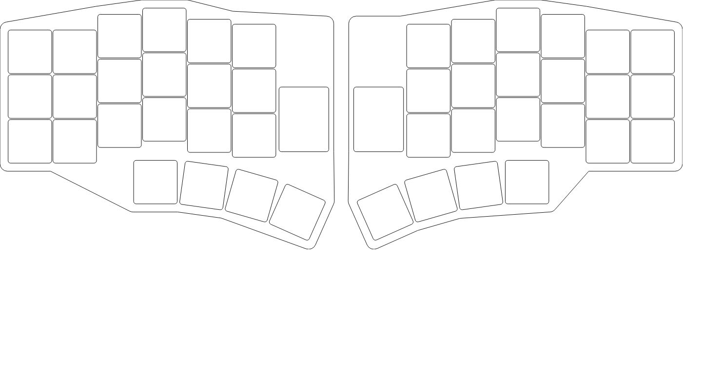 | 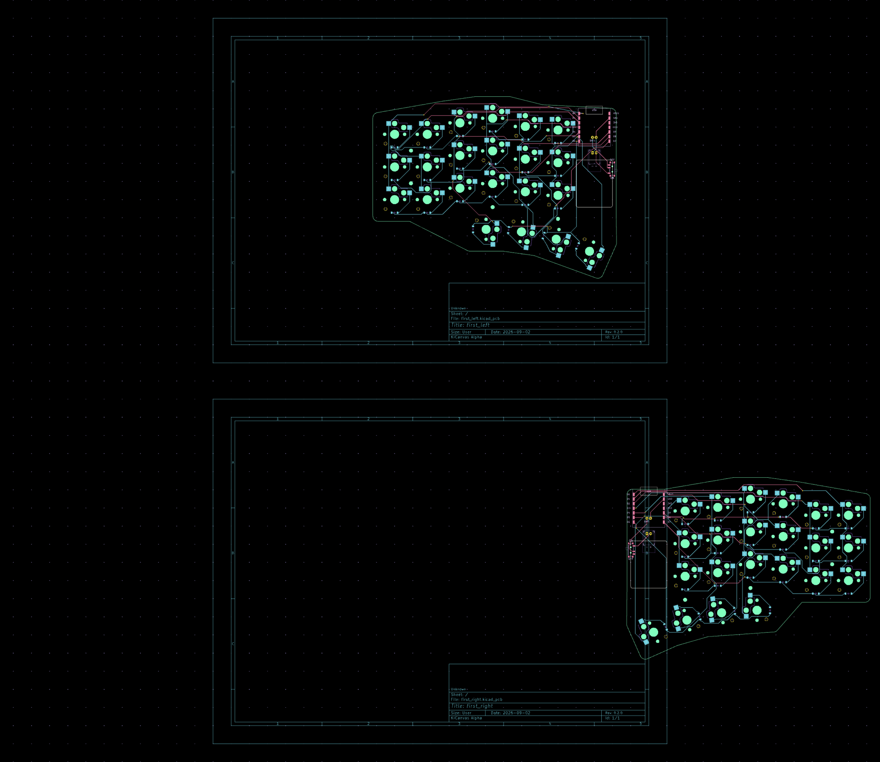 |
kicad/first_left.kicad_pcb / kicad/first_right.kicad_pcb — 配線済み・DRC 違反 0・未配線 0gerbers/first_left.zip / gerbers/first_right.zip — 発注用ガーバー(JLCPCB 等にそのままアップロード可)npm install # ergogen をローカルにインストール
npm run build # = ergogen . --clean → output/ に未配線 PCB を再生成
npm run build:svg # 外形 SVG も出力注意:
output/はビルドのたびに完全に上書きされます。配線済みデータはkicad/、 発注データはgerbers/にあり、これらはビルドでは消えません。config を変更したら 「npm run build→output/pcbs/*.kicad_pcbをkicad/にコピー → 再ルーティング」が必要です。
.
├── config.yaml              Ergogen 設定 = 回路の一次ソース (キー配置・外形・ネット定義)
├── footprints/
│   ├── ceoloide/            ceoloide/ergogen-footprints (Choc, ダイオード, JST, 電源SW 等) ※CC BY-NC-SA 4.0
│   └── local/mcu_xiao_nrf52840_plus.js   XIAO nRF52840 Plus (Seeed 公式 KiCad データの座標から作成)
├── output/                  Ergogen 生成物 (未配線。ビルドごとに上書き)
├── kicad/                   配線済み PCB (Freerouting + 手修正、DRC クリーン)
├── gerbers/                 発注用ガーバー zip
└── docs/ プレビュー画像outer, pinky, ring, middle, index, inner、行は下から bottom, home, top。
Columnar stagger は pinky 基準で ring +6.3 / middle +8.8 / index +4.3 / inner +2.3 mm。
親指 4 キーは rotate: -90、半径 140mm の円弧上に 8° ピッチで扇状配置。first_left) と右手用 (first_right) を別々に生成・配線しています。&xiao_d n)
| 用途 | ピン |
|---|---|
| 列 outer→inner | D0 D1 D2 D3 D4 D5 |
| 親指 t1→t4 | D2 D3 D4 D5 (列を流用) |
| 行 top / home / bottom / thumb | D9 / D8 / D7 / D6 |
| 電源 | JST(BAT_P) → 電源SW → VBAT (モジュール裏パッド、基板のスルーホール経由で半田付け) |
| リセット | XIAO 本体ボタン (1回=リセット、素早く2回=ブートローダ) |
| 空き | D10 (+ Plus 裏面の D11〜D19) |
gerbers/first_left.zip をアップロード → 2層 / 1.6mm / 1oz / HASL でそのまま注文 (最低5枚)first_right.zip も同様に注文 (別設計扱い)回路図ファイル (.kicad_sch) は存在しません。config.yaml が回路図に相当する一次ソースで、
接続定義 (from/to) はすべてそこに書かれています。回路を変更するときは config を編集して再生成し、
Freerouting で再ルーティングします (このリポジトリの履歴と配線図ドキュメントを参照)。
| Qty | Value | Footprint | References |
|---|---|---|---|
| 22 | ceoloide:switch_choc_v1_v2 | S1, S2, S3, S10, S11, S12, S13, S14, S15, S16, S17, S18, S19, S20, S21, S22 +6 | |
| 22 | ceoloide:diode_tht_sod123 | D1, D2, D3, D10, D11, D12, D13, D14, D15, D16, D17, D18, D19, D20, D21, D22 +6 | |
| 4 | ceoloide:mounting_hole_npth | MH1, MH2, MH3, MH4 | |
| 1 | ceoloide:power_switch_smd_side | PWR1 | |
| 1 | local:mcu_xiao_nrf52840_plus | MCU1 | |
| 1 | ceoloide:battery_connector_jst_ph_2 | JST1 |
davidphilipbarr/Sweep
Sweep - a small promicro based keyboard inspired by the Ferris.


W0rthlessS0ul/nRF24_jammer
The nRF24 jammer is a powerful tool that requires an ESP32 and configurable numbers of NRF24 modules to assemble.

hackclub/OnBoard
💡 Join 1,000 teenagers and make your first PCB with a $100 grant!


Neumi/open_echo
Open Source echo sounder / depth sounder / SONAR for bathymetry and research. Arduino based and compatible.


vsfteam/vsf
Versaloon Software Framework -- a tiny preemptive-capable event-driven incremental software framework for embedded systems
It measures 134.2 × 100 mm and has 2 copper layers, 1.6 mm thick.
51 parts. The full list of its parts is on this page, with links to each part's symbol and footprint where PCBKit's library has them.
From the sunda-eimami/ULTRA_KEYBOARDS repository on GitHub, at the commit this page was made from: the board is kicad/first_left.kicad_pcb. PCBKit opens the board in the browser, with nothing to install.
Its repository states no licence, so its author keeps all rights: ask sunda-eimami before reusing the design.