


2 layers333.4 × 149.9 mm

 SukkoPera/16up13
User Port Cartridge for the Commodore 16, 116 and Plus/4
16up is an open-source printed circuit board by SukkoPera, from the SukkoPera/16up repository on GitHub. It is a 2-layer board of 60.8 × 85 mm with 20 parts on 85 nets, routed with 737 tracks and 52 vias.
It is built around the 74HCT04D. Its parts include 5 ICs, 4 capacitors, 4 connectors, 2 resistors and 1 crystal. It belongs with the retro computing and games boards of this library.
16UP is an Open Hardware Expansion board that will add a User Port to the Commodore 16, 116 and Plus/4 home computers.
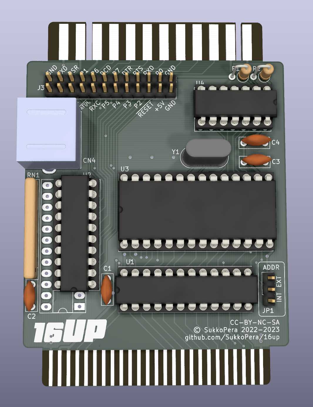
The biggest difference between the Commodore 16/116 and the Plus/4, besides the different amount of RAM installed, is that the former lacks a User Port. In the past there were numerous attempts at making a cartridge for the Expansion Port that would fill this gap, but apparently none of them succeeded...
... None of them except this project, of course! :) 16UP will plug into the Expansion Port and "convert" it to a User Port that will be mostly compatible with that featured on the Plus/4. It can also be used on a Plus/4 in order to gain an extra User Port.
If you are interested in this board, please read this document carefully, there are a few aspects that you must be aware of.
There are currently two usable versions of 16UP:
Both versions are valid and fully working, it is up to the user to choose what is best for them.
Both versions of 16UP can be configured to respond to two different address sets through the JP1 jumper:
This configuration will expose the ACIA (Serial port) at address $fd6x and the MOS 6529 (Parallel port) at $fd7x. These addresses are normally unused in both the C16/116 and +4, thus this setting is the most compatible, but it will need "special" software that either looks for the ports at these addresses or that allows the addresses to be configured manually.
On a +4, this configuration will effectively add a second User Port that can be used independently of the built-in one.
This configuration will expose the ACIA and MOS 6529 at the same addresses that are normally used on a +4 ($fd0x for the ACIA and $fd10 for the 6529). Of course this means that it cannot be used on a +4 as the port would conflict with the built-in one. It is rather meant to be used on a C16/116, making it ALMOST (see below) compatible with all the +4 software that uses the User Port.
NOTE: Using this board on a C16/116 requires an internal modification in the machine. While this may sound impractical, it is fairly easy to perform and there are good reasons to perform it even if you are not interested in using this board. Please see this page for details.
If you perform the C16/116 modification, plug 16UP in the Expansion Port and want to use the Datassette, you will notice that the computer will no longer detect when you press Play upon the Press Play on tape prompt. This is absolutely normal and is actually a sign that the modification works as intended. If you really want to use the Datassette you can either remove the board from the Expansion Port or make a Y cable with one female and two male MiniDIN-7 connectors: the Datassette will plug into the female connector, while one of the two male ones will plug into the C16/116 and the other one into the MiniDIN-7 connector on the 16up board.
Hint: if you want to save wire and effort, it is enough to bring the Sense signal (Pin 6) to the connector that plugs into 16UP.
Another hint: if you use one of these instead of the female connector, you can make an adapter for the C64 (1530) Datassette ;).
Since all the serial signals are handled on-board, they are not brought out to the edge connector. Any peripheral that uses any signals besides P1-P8, /ATTN and /RESET just won't work with V2 and that's why V3 was developed.
The +4 User Port is made up of a few distinct elements, let's analyze them one by one:
The 8-bit parallel port can be implemented by a few different hardware components and is fully functional. There are a few caveats though:
(Do not blame me for the above, these are questionable design decisions straight from Commodore and those problems also affect a real +4.)
The +4 User Port has all the signals required by an RS-232 interface, but they are at TTL voltage levels (i.e.: 0/+5V). This is fine if you need to connect a microcontroller like an Arduino but in order to turn them into a real RS-232 port, they need to be shifted to higher voltages.
As already mentioned, you will need to use an extra adapter that plugs into the User Port edge connector.
16UP V2 has such an adapter built-in and thus features a full RS-232 port on the onboard DE-9 connector.
All signals on the port are connected and usable, with the exception of Ring Indicator. DCD, DSR and /CTS are pulled to the asserted level in order to allow communication with devices/cables that do not use those signals.
When using the serial port, you must decide whether you want hardware flow control to be handled by the ACIA or by the KERNAL: this might sound odd but it is due to the fact that ACIA chips of the era have an hardware bug that causes the /CTS signal to be handled incorrectly. Commodore engineers must have found that out and decided to let the KERNAL handle it (if you look at the +4 schematics, you can clearly see that the signal was rerouted at a later stage). You can make your choice through the JP2/JP3 jumpers (always move them both to the same side!): the SW setting will pass /CTS to the KERNAL and is the recommended one as this is the configuration used on the +4. The HW position is only recommended if you are using a W65C51S chip (which should have fixed the bug) and is mainly meant as an experimental feature.
If you are looking for a terminal emulator, I recommend Term-80 as it is hands down the most feature-rich program of its kind (Hint: press CBM+HELP when you get lost) and supports communication at 19200 bps (Take that, C64!).
This is fully functional as on the original +4.
The /ATTENTION signal is not present on the C16/116 Expansion Port. Thus, if you need it, you will need to provide the board with it through the /ATTN (J1) connector on V2 or through the relevant pin of the J3 pin header on V3. The signal is available on pin 3 of the IEC (Serial) port and it can be connected in parallel to any other device you already have on that port, just break it out.
This is directly connected to the main power rails of the C16/116. Use common sense and do not draw "too much" power out of it.
This is not present on the C16/116 Expansion Port and thus the corresponding pins of the User Port are left unconnected on V2, while on V3 they can be powered from the relevant pins of the J3 pin header. This should not be a big deal though, as the main use case for this is to provide the higher voltages needed for a fully-compliant RS-232 interface but 16UP V2 has that built-in in a way that does not require an actual higher-voltage supply, and the same applies for the recommended adapter for V3. Let me know if you find any User Port peripherals that require it.
The parallel port on the +4 is driven through a MOS 6529 (U2 on the board). Since these days that IC is pretty hard to get hold of, an alternative circuit based on a 74LS654 was designed by Daniël Mantione and integrated into the board. Depending on what you choose to use:
There are various ICs that can be used as ACIA (U3):
The board uses a GAL for address decoding. Either a GAL20 or GAL22 can be used and both can be programmed with the ubiquitous TL866 programmers. The required JED files can be found in the relevant directories. The GAL speed shouldn't matter too much, I used a 25ns model with no particular issues.
The 16UP documentation, including the design itself, is copyright © SukkoPera 2022-2023 and is licensed under the Creative Commons Attribution-NonCommercial-ShareAlike 4.0 International License.
This documentation is distributed as is and WITHOUT ANY EXPRESS OR IMPLIED WARRANTIES whatsoever with respect to its functionality, operability or use, including, without limitation, any implied warranties OF MERCHANTABILITY, SATISFACTORY QUALITY, FITNESS FOR A PARTICULAR PURPOSE or infringement. We expressly disclaim any liability whatsoever for any direct, indirect, consequential, incidental or special damages, including, without limitation, lost revenues, lost profits, losses resulting from business interruption or loss of data, regardless of the form of action or legal theory under which the liability may be asserted, even if advised of the possibility or likelihood of such damages.
If you want to get some boards manufactured, you can get them from PCBWay through this link:

You get my gratitude and cheap, professionally-made and good quality PCBs, I get some credit that will help with this and other projects. You won't even have to worry about the various PCB options, it's all pre-configured for you!
Also, if you still have to register, you can use this link to get some bonus initial credit (and yield me some more).
You can also buy me a coffee if you want:

Inspiration for this board came from an uncompleted project by Solder/Synergy.
Other people from the Plus/4 World Forum helped, in particular:
| Qty | Value | Footprint | References |
|---|---|---|---|
| 4 | 100n | Capacitor_THT:C_Disc_D7.0mm_W2.5mm_P5.00mm | C1, C2, C3, C4 |
| 2 | 10k | Resistor_THT:R_Axial_DIN0207_L6.3mm_D2.5mm_P2.54mm_Vertical | R1, R2 |
| 1 | 1.8432M | Crystal:Crystal_HC49-U_Vertical | Y1 |
| 1 | 74HCT04 | Package_DIP:DIP-14_W7.62mm_Socket_LongPads | U4 |
| 1 | 74LS654 | Package_DIP:DIP-24_W7.62mm_Socket_LongPads | U102 |
| 1 | 8.2k | Resistor_THT:R_Array_SIP9 | RN1 |
| 1 | ALMOST_USERPORT | 16up:Plus4_UserPort | CN2 |
| 1 | CC-BY-NC-SA | 16up:cc_by_nc_sa | V1 |
| 1 | CONN_UPORT254 | Connector_PinHeader_2.54mm:PinHeader_2x12_P2.54mm_Vertical | CN3 |
| 1 | EXPANSION_PORT | 16up:C16_Cart_Conn | CN1 |
| 1 | GAL20V8 | Package_DIP:DIP-24_W7.62mm_Socket_LongPads | U1 |
| 1 | JMP_ADDRESS | Connector_PinHeader_2.54mm:PinHeader_1x03_P2.54mm_Vertical | JP1 |
| 1 | LOGO | 16up:logo | V0 |
| 1 | MOS_6529 | Package_DIP:DIP-20_W7.62mm_Socket_LongPads | U2 |
| 1 | MOS_6551_ACIA | Package_DIP:DIP-28_W15.24mm_Socket_LongPads | U3 |
| 1 | TAPE_IN | 16up:KMDGX-7S-BS | CN4 |
It measures 60.8 × 85 mm and has 2 copper layers, 1.6 mm thick.
20 parts, built around the 74HCT04D. The full list of its parts is on this page, with links to each part's symbol and footprint where PCBKit's library has them.
From the SukkoPera/16up repository on GitHub, at the commit this page was made from: the board is 16up.kicad_pcb. PCBKit opens the board in the browser, with nothing to install.
Its repository states no licence, so its author keeps all rights: ask SukkoPera before reusing the design.


tebl/RC6502-Apple-1-Replica
An expandable SBC-version of the Apple 1 computer, easy to get started with and lot of cool stuff that can be added to it!


leomil72/LM80C
A Z80-based homebrew computer withTMS9918, AY-3-8910, Z80 CTC, Z80 PIO, and Z80 SIO

DoctorWkt/CSCvon8
A crazy small 8-bit CPU built with only seventeen 7400-series chips.

RichardRozehnal/Gotek-Floppy-Disk-Emulator-V2
Floppy disk emulator for old computers and machines, Amiga, Atari ST, etc.

michalin/TMS9918_Arduino
8-bit retro graphic card with TMS9918 and Arduino library