
4 layers53 × 39.5 mm
 suikan4github/Akashi-13
Ethernet / CF JIG for Nucleo H743ZG2
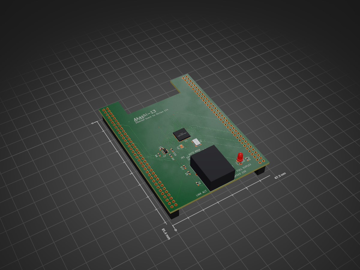
Akashi-13 is an open-source printed circuit board by suikan4github, from the suikan4github/Akashi-13 repository on GitHub, published under the MIT licence. It is a 4-layer board of 67.3 × 91.4 mm with 38 parts on 149 nets, routed with 769 tracks and 95 vias.
It is built around the LAN9220-ABZJ. Its parts include 18 capacitors, 12 resistors, 3 connectors, 2 ICs and 1 diode.
Ethernet JIG for Nucleo H743ZI2
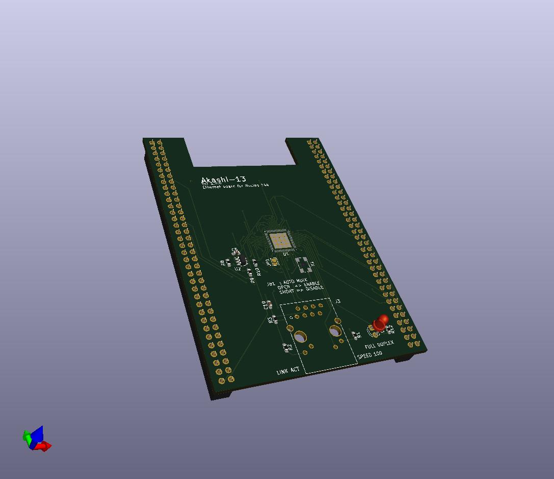
This is a LAN9220 ehternet controller board for the Nucleo H743ZI.
The LAN9220 is accessible through the FMC SRAM configuration NE1. The LAN9220 doesn't have READY signal. Thus, the wait cycles should be set by program appropriately.
The following signals could be assigned to the interrupt (EXTI).
The followings are the pin configuration of Nucleo board.
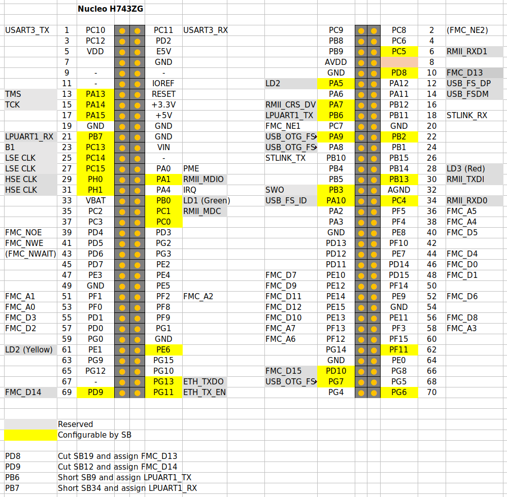
Also, short bridge have to be configured as the followings :
The USART3 is connected to STLINK VCOMM through the PD8 and PD9 by default. These pins are re-assigned to FMC. Thus, the LPUART1 have to be connected to the STLINK VCOMM through the PB6 and PB7.
PD6 (FMC_NWAIT) and FMC_NE1 (PC7) are not used in this board.
This project is licensed by the MIT license.
| Qty | Value | Footprint | References |
|---|---|---|---|
| 6 | 0.1u | Capacitor_SMD:C_0603_1608Metric_Pad1.08x0.95mm_HandSolder | C5, C6, C8, C10, C12, C13 |
| 6 | 4.7u | Capacitor_SMD:C_0603_1608Metric_Pad1.08x0.95mm_HandSolder | C7, C11, C14, C15, C16, C17 |
| 4 | 15p | Capacitor_SMD:C_0603_1608Metric_Pad1.08x0.95mm_HandSolder | C1, C2, C3, C4 |
| 4 | 50 | Resistor_SMD:R_0603_1608Metric_Pad0.98x0.95mm_HandSolder | R4, R5, R6, R7 |
| 3 | 300 | Resistor_SMD:R_0603_1608Metric_Pad0.98x0.95mm_HandSolder | R1, R2, R12 |
| 2 | 10k | Resistor_SMD:R_0603_1608Metric_Pad0.98x0.95mm_HandSolder | R8, R10 |
| 2 | Conn_02x35_Odd_Even | Connector_PinSocket_2.54mm:PinSocket_2x35_P2.54mm_Vertical | J1, J2 |
| 1 | 0.022u | Capacitor_SMD:C_0603_1608Metric_Pad1.08x0.95mm_HandSolder | C19 |
| 1 | 10 | Resistor_SMD:R_0603_1608Metric_Pad0.98x0.95mm_HandSolder | R3 |
| 1 | 10u | Capacitor_SMD:C_0603_1608Metric_Pad1.08x0.95mm_HandSolder | C9 |
| 1 | 12.4k | Resistor_SMD:R_0603_1608Metric_Pad0.98x0.95mm_HandSolder | R11 |
| 1 | 4.7k | Resistor_SMD:R_0603_1608Metric_Pad0.98x0.95mm_HandSolder | R9 |
| 1 | 93AA46AT-IOT | Package_TO_SOT_SMD:SOT-23-6 | U2 |
| 1 | CONN12_011D01BNL_PUL | MyFootprint:J0011D01BNL | J3 |
| 1 | DFA-S15 | Oscillator:Oscillator_SMD_Fordahl_DFAS15-4Pin_5.0x3.2mm | X1 |
| 1 | LAN9220-ABZJ | Package_DFN_QFN:QFN-56-1EP_8x8mm_P0.5mm_EP5.9x5.9mm | U1 |
| 1 | LED | LED_THT:LED_D3.0mm | D1 |
| 1 | SolderJumper_2_Open | Jumper:SolderJumper-2_P1.3mm_Open_TrianglePad1.0x1.5mm | JP1 |
It measures 67.3 × 91.4 mm and has 4 copper layers, 1.6 mm thick.
38 parts, built around the LAN9220-ABZJ. The full list of its parts is on this page, with links to each part's symbol and footprint where PCBKit's library has them.
From the suikan4github/Akashi-13 repository on GitHub, at the commit this page was made from: the board is Akashi-13.kicad_pcb and its schematic Akashi-13.kicad_sch. PCBKit opens the board in the browser, with nothing to install.
Its repository publishes it under the MIT licence: you may reuse it on that licence's terms (keep the author's notice, and for a copyleft licence share your changes alike).
Hanqaqa/Easyduino
Easily dive into different PCB KiCad designs of the most popular microcontroller devboards

murexrobotics/electrical
Highly integrated electronics design and printed circuit boards (PCBs) for the MATE ROV Competition. Attempt the impossible.


magnusnordlander/smart-lcc
A smarter LCC for the Lelit Bianca V2, with Wi-Fi and stuff.

Roboy/HTC_Vive_Sensors
Schematics and PCB designs for our custom Vive sensors based on a quad op-amp chip rather than discrete transistors.

sparkfun/SparkFun_RTK_Facet
The hardware and enclosure for the popular centimeter level RTK Facet GNSS receiver with built in display.
