2 layers18 × 16.5 mm

 str-dst/simplified-daughterboard26
A simple USB daughterboard
SDB panel is an open-source printed circuit board by str-dst, from the str-dst/simplified-daughterboard repository on GitHub, published under the CC-BY-SA-4.0 licence. It is a 2-layer board of 48 × 35 mm with 148 parts on 36 nets, routed with 244 tracks and 24 vias.
Its parts include 8 resistors, 8 connectors, 4 diodes and 4 inductors.
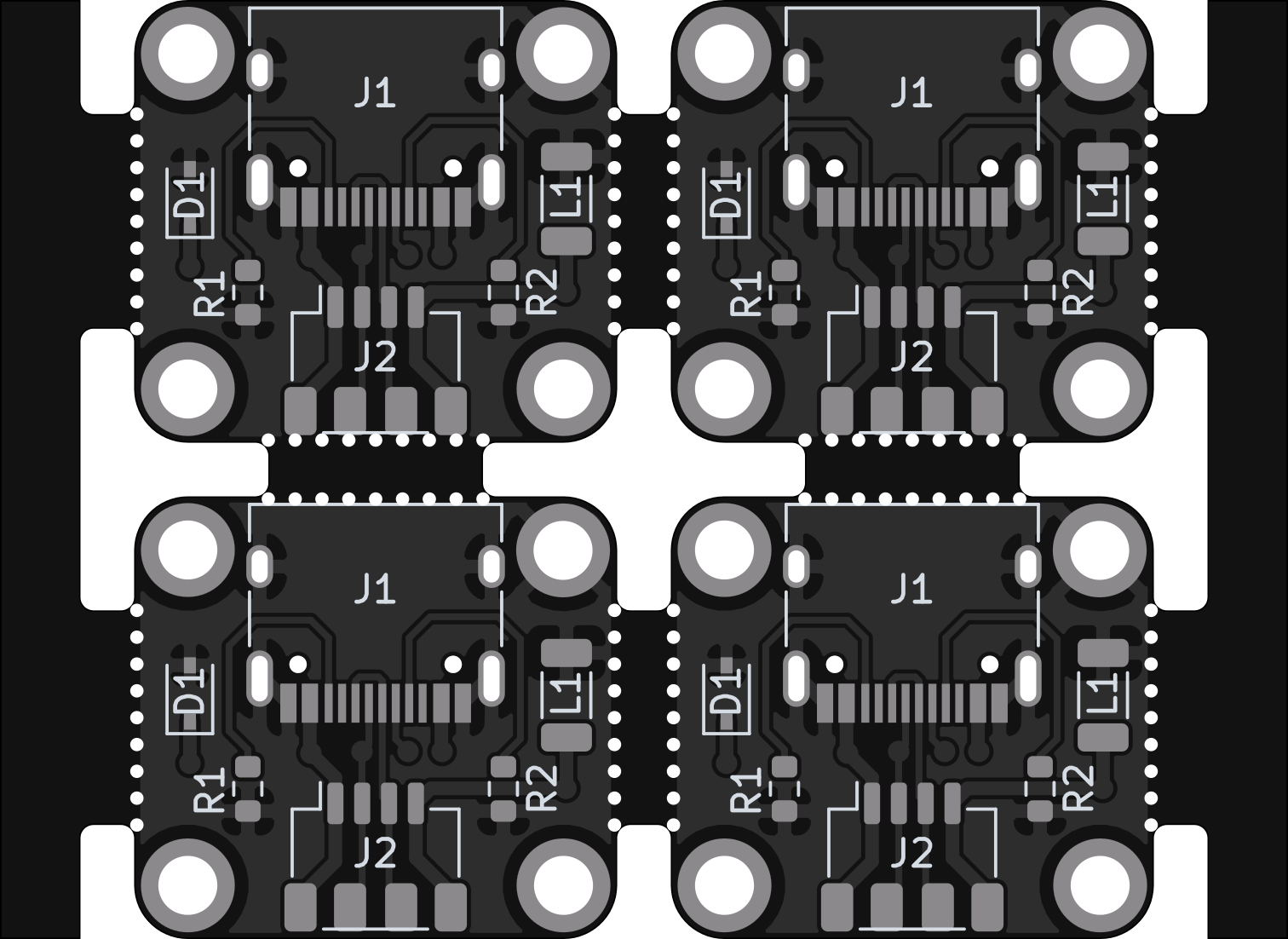
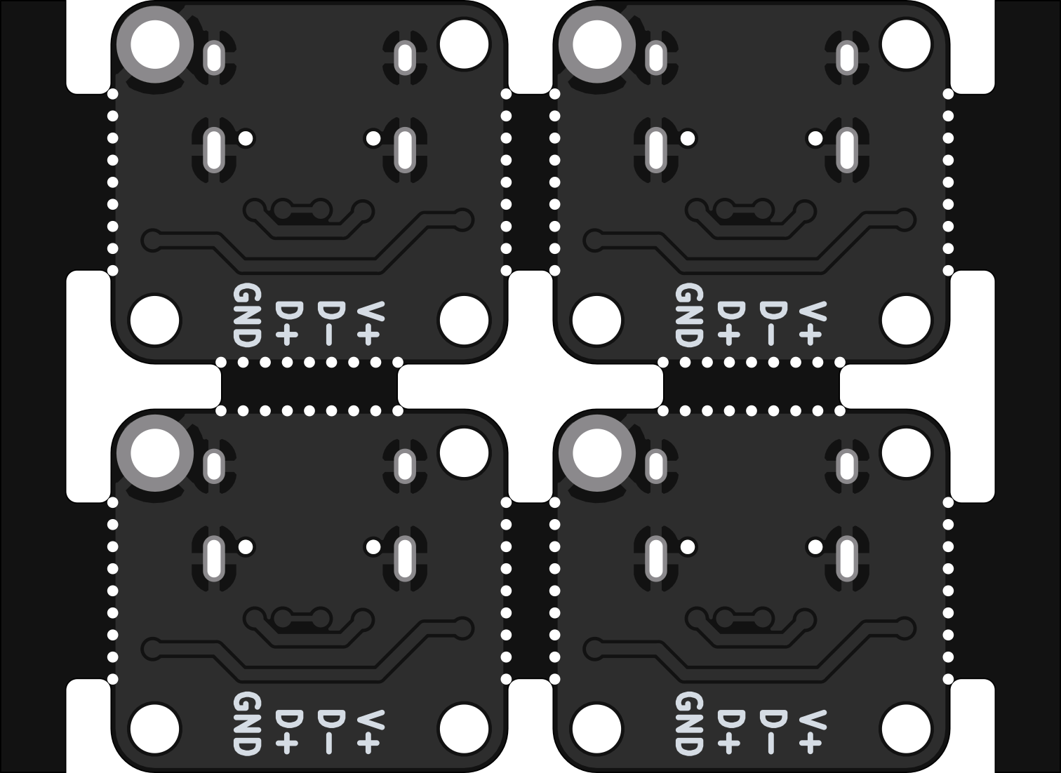
| Qty | Value | Footprint | References |
|---|---|---|---|
| 12 | MountingHole | custom_parts:Generic-Mounthole | H2, H2, H2, H2, H3, H3, H3, H3, H4, H4, H4, H4 |
| 8 | 5.6k | Resistor_SMD:R_0603_1608Metric | R1, R1, R1, R1, R2, R2, R2, R2 |
| 4 | Conn_01x04 | custom_parts:JST_SH_SM04B-SRSS-TB_1x04-1MP_P1.00mm_Horizontal | J2, J2, J2, J2 |
| 4 | D_TVS | Diode_SMD:D_SOD-323 | D1, D1, D1, D1 |
| 4 | L_Core_Ferrite | Inductor_SMD:L_1206_3216Metric | L1, L1, L1, L1 |
| 4 | MountingHole_Pad | custom_parts:Generic-Mounthole-dual | H1, H1, H1, H1 |
| 4 | USB_C_Receptacle_USB2.0 | Connector_USB:USB_C_Receptacle_HRO_TYPE-C-31-M-12 | J1, J1, J1, J1 |
The 40 most common of 148 parts.

nasa-jpl/open-source-rover
A build-it-yourself, 6-wheel rover based on the rovers on Mars!


peej/rosaline-keyboard
40% staggered through-hole component keyboard PCB for standard 60% cases


OpenA3XX/opena3xx-panel-design
OpenA3XX: Panels, 3D Printed Components & Reference Archive
It measures 48 × 35 mm and has 2 copper layers, 1.6 mm thick.
148 parts. The full list of its parts is on this page, with links to each part's symbol and footprint where PCBKit's library has them.
From the str-dst/simplified-daughterboard repository on GitHub, at the commit this page was made from: the board is fab/sDB_panel.kicad_pcb. PCBKit opens the board in the browser, with nothing to install.
Its repository publishes it under the CC-BY-SA-4.0 licence: you may reuse it on that licence's terms (keep the author's notice, and for a copyleft licence share your changes alike).