2 layers49.4 × 35.8 mm
WS2812Controller
klein0r/pcb-ws2812-wifi-controller
WiFi Controller for WS2812 LED Stripes
22 parts82MIT

 str-dst/feinstaub8
piggyback PCB for the SDS011 sensor
Feinstaub is an open-source printed circuit board by str-dst, from the str-dst/feinstaub repository on GitHub, published under the CC-BY-SA-4.0 licence. It is a 2-layer board of 67.1 × 62.2 mm with 14 parts on 16 nets, routed with 303 tracks and 0 vias.
It is built around the ESP-12F and AMS1117-3.3. Its parts include 4 resistors, 3 ICs, 3 connectors, 1 capacitor and 1 switch. It belongs with the sensors and measurement boards and the ESP8266 boards of this library.


The board is designed to run with the luftdaten.info firmware and has a place for a BME280 sensor.
Pic of the prototype (with enamel wire because it wouldn't be a prototype without it).

| Count | Part | Reference | Part URL |
|---|---|---|---|
| 1 | ESP12-F | U1 | ESP-12F |
| 1 | Bosch BME-280 module | U2 | BME280 |
| 1 | Nova Fitness SDS-011 Module | --- | SDS-011 |
| 1 | AMS1117-3.3v step-down module | U3 | AMS1117-3.3 module |
| 1 | DIP switch | SW1 | DIP-Switch |
| 1 | 100 nF ceramic disk capacitor | C1 | Kemet C315C104M5U5TA |
| 4 | 10 kΩ resistor | R1-R4 | Multicomp MF25 10k |
The SDS011 module gets connected to the J2 pins on the main PCB.
Remember that TX and RX have to be connected in reverse on the module.
The ESP chip can be flashed by connecting an ISP flasher to the J1 pins.
To put the chip into flashing mode set the boot switch to on, plug in the power and then turn the switch back off.
The easiest method of flashing the chip is by using the AirRohr firmware updater
For the main power input a 5v / 0.5-1A power supply should be used.
DO NOT CONNECT BOTH THE MAIN POWER AND A USB FLASHER WITH POWER INPUT AT ONCE!!!
If you use a flashing device that has 3.3v power output on it's own the main power has to be left unconnected.
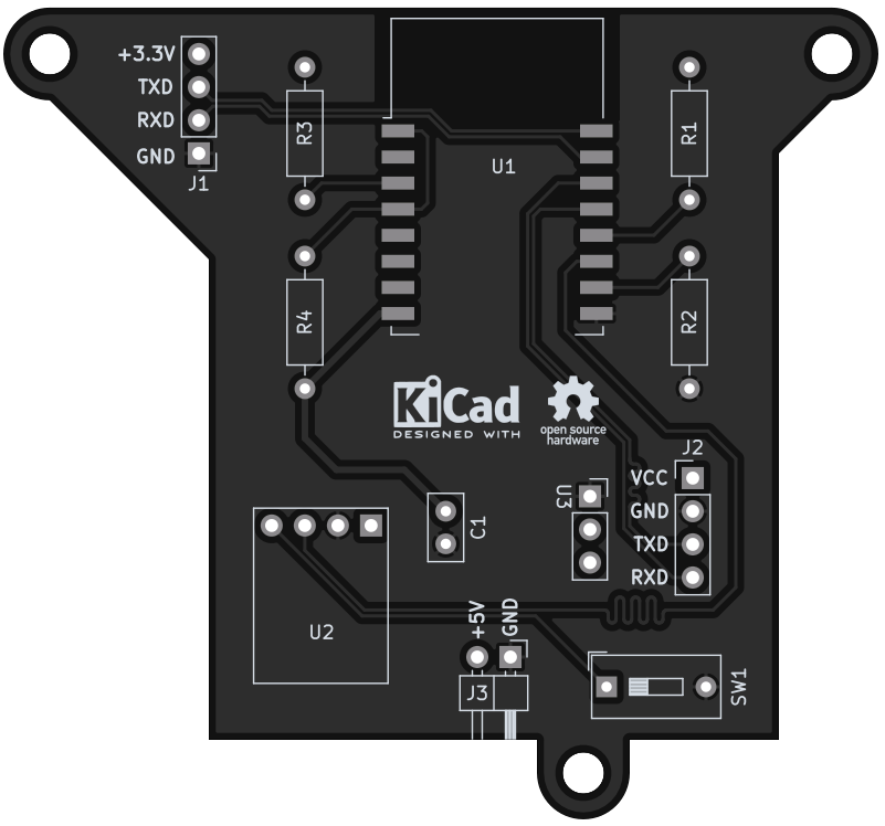
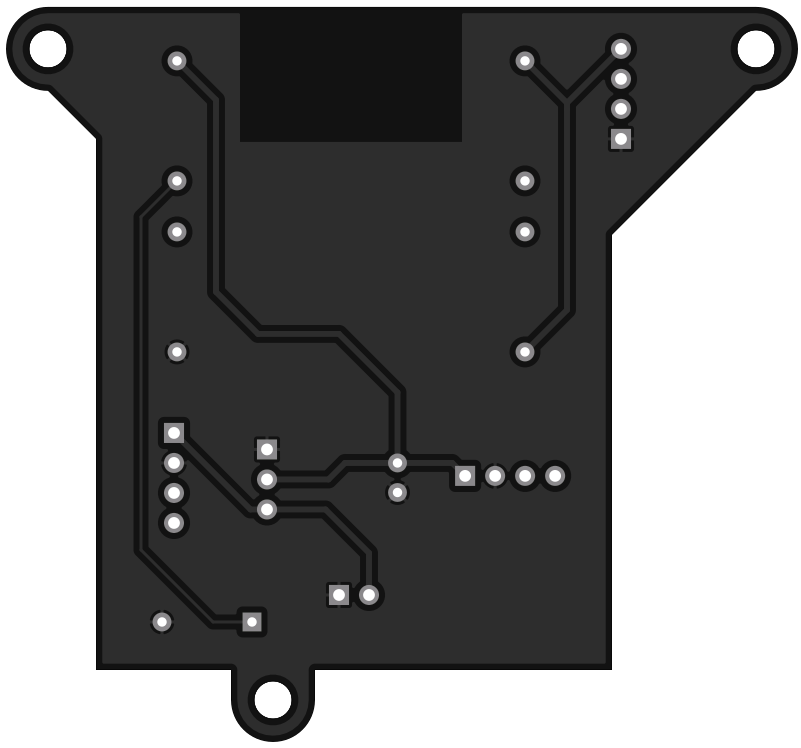
This work is licensed under a Creative Commons Attribution-ShareAlike 4.0 International License.

| Qty | Value | Footprint | References |
|---|---|---|---|
| 4 | 10K | Resistor_THT:R_Axial_DIN0207_L6.3mm_D2.5mm_P10.16mm_Horizontal | R1, R2, R3, R4 |
| 2 | Conn_01x04 | Connector_PinHeader_2.54mm:PinHeader_1x04_P2.54mm_Vertical | J1, J2 |
| 1 | AMS1117-3.3 | Connector_PinSocket_2.54mm:PinSocket_1x03_P2.54mm_Vertical | U3 |
| 1 | C | Capacitor_THT:C_Disc_D5.0mm_W2.5mm_P2.50mm | C1 |
| 1 | Conn_01x02 | Connector_PinHeader_2.54mm:PinHeader_1x02_P2.54mm_Horizontal | J3 |
| 1 | ESP-12F | custom_parts:ESP-12F | U1 |
| 1 | LOGO | custom_parts:oshw | G*** |
| 1 | LOGO | custom_parts:kicad | G*** |
| 1 | SW_DIP_x01 | Button_Switch_THT:SW_DIP_SPSTx01_Slide_9.78x4.72mm_W7.62mm_P2.54mm | SW1 |
| 1 | bme280_module | custom_parts:bme280 | U2 |
It measures 67.1 × 62.2 mm and has 2 copper layers, 1.6 mm thick.
14 parts, built around the ESP-12F and AMS1117-3.3. The full list of its parts is on this page, with links to each part's symbol and footprint where PCBKit's library has them.
From the str-dst/feinstaub repository on GitHub, at the commit this page was made from: the board is feinstaub.kicad_pcb and its schematic feinstaub.kicad_sch. PCBKit opens the board in the browser, with nothing to install.
Its repository publishes it under the CC-BY-SA-4.0 licence: you may reuse it on that licence's terms (keep the author's notice, and for a copyleft licence share your changes alike).
klein0r/pcb-ws2812-wifi-controller
WiFi Controller for WS2812 LED Stripes


klein0r/pcb-ttl-ftdi-esp-adapter
PCB to connect a TTL reader either to an FTDI or ESP12-E/F (WiFi)


piwko28/smart-home-ebus-adapter
eBUS adapter PCB for use with ebusd-esp firmware as well as with other UART devices.


alextrical/ESP8266-Sentinel-Kinetic-Wired-Remote
ESP8266 based Re-implementation of the Vent-Axia Sentinel Kinetic Wired Remote Controller
