2 layers59.2 × 52.9 mm
 stepleton/SLT_interconnect1
Wire-to-board power interconnect for the IBM SLT card modular system
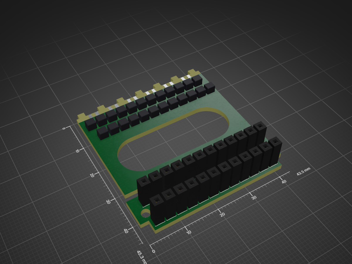
SLT interconnect is an open-source printed circuit board by stepleton, from the stepleton/SLT_interconnect repository on GitHub, published under the Unlicense licence. It is a 2-layer board of 43.5 × 45.3 mm with 57 parts on 24 nets, routed with 163 tracks and 0 vias.
This project aims to construct a modern replacement for the wire-to-board connectors that IBM used inside some products incorporating their proprietary Solid Logic Technology (SLT) and Monolithic System Technology (MST) circuit design systems. The design has features like wide circuit board traces intended to make it suitable for use as a power connector, but there's no reason it couldn't be used for logic interconnect as well.
This hardware design and all other materials distributed alongside it are made available for free with NO WARRANTY OF ANY KIND. Any system that interfaces with hardware built from this design could suffer malfunction, data loss, physical damage, or other harms. Some of these effects could be permanent and/or unrepairable. If you're not prepared to risk these consequences, don't use these resources.
Most people familiar with SLT and MST will think of the square aluminium housings for hybrid circuits and ICs (respectively) that appeared on IBM components from the 1960s through the 1990s. As it happens, SLT and MST specifications also described ways of building circuit boards and connecting them together. SLT and MST-based components saw widespread use in IBM products, from typewriters to large mainframe computers.
SLT and MST's most common methods of interconnect were based on 24-pin header-style connectors. "Plugs" (my terminology) were simply made from two rows of twelve individual metal pins embedded in a circuit board; these were usually found on boards meant to connect other boards together, like backplanes. "Sockets" that mated with these plugs were formed from metal spring contacts lined up on the edges of circuit boards and surrounded by a plastic shroud; these were usually found on modular cards that held electronic components (ICs, resistors, etc.). They could also appear on wire-to-board connectors, where multiple wires or a flat ribbon cable would be soldered directly to a small circuit board with an integrated socket connector on one edge.
This blog post presents a good illustrated overview of SLT and MST cards and their connectors. As it notes, the unusual arrangement of 1/8-inch (3.175mm) spacing between pins on the same row, plus the 1/4-inch (6.35mm) spacing between rows, is incompatible with common header connectors manufactured today.
Lacking off-the-shelf options for SLT and MST interconnect, we can arrange modern components in a way that is compatible with the IBM designs.
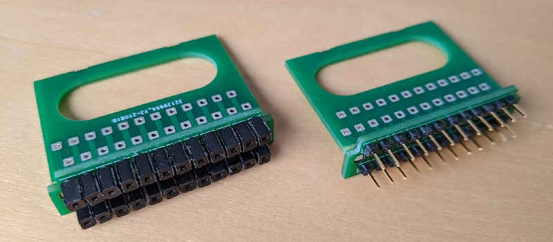
Figure 1. Our wire-to-board adaptor is economically constructed from two small circuit boards joined together perpendicularly, and from single-pin header pins and sockets arranged according to the 1/8-inch (3.175mm) and 1/4-inch (6.35mm) spacing requirements.
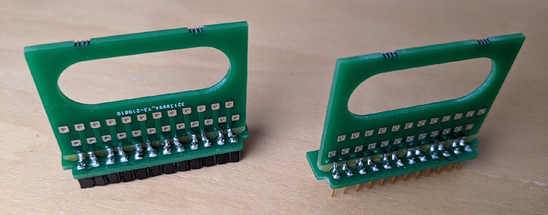
Figure 2. The two circuit boards are "glued" together by solder joints that also connect the connector header pins and sockets to the plated through-holes where wires will terminate. Threading the wires through an oval-shaped hole on the vertical circuit board can help them stay tidy and may offer some amount of strain relief. The mechanical strength of the solder-bonded joint between the circuit boards is considerable, and most applications are unlikely to require additional reinforcement there.
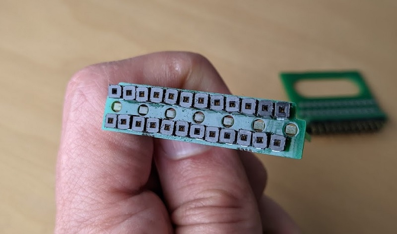
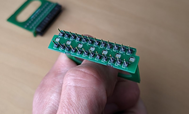
Figure 3. The nonstandard pin spacing makes it a bit tricky to ensure a tidy alignment of the constituent pins and sockets, especially if these parts are made by trimming breakaway or cuttable strips and therefore vary in size. Perfection may be impossible, but persistence can give you a functional arrangement that orients square pins and square sockets to align roughly with the board itself. Note that like the plastic shroud on the original IBM socket connector, the connector's horizontal circuit board is also polarised by square notches in two of its corners.
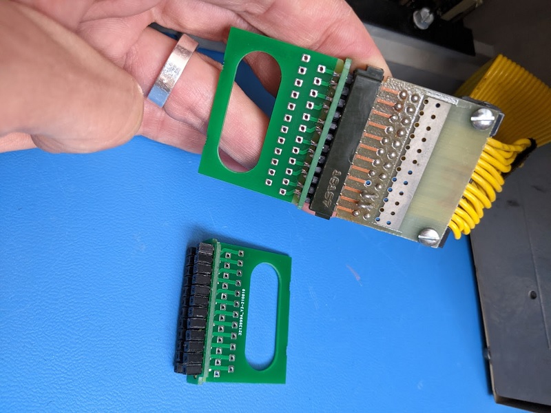
Figure 4. The plug adaptor can mate with an original IBM SLT/MST socket, like the one on this wire-to-board power connector from an IBM 5100 portable computer. It's not clear that this arrangement would be reliable without an additional means of securing the connectors together: by wiggling both of them around the connection as if it were a hinge, they can come apart fairly easily.
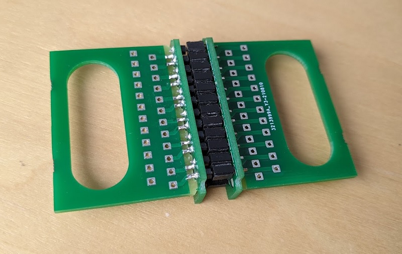
Figure 5. Naturally, the plug and socket adaptors can connect to each other, but the same caveat about security applies.
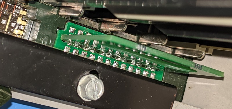
Figure 6. When made with low-profile pin sockets, the socket adaptor can fit into the same places where real IBM wire-to-board socket adaptors go. Like the IBM original, our adaptor is liable to come loose of the plug unless it is restrained somehow. For this, the IBM 5100 makes use of a metal bracket coated in a non-conductive black enamel finish.
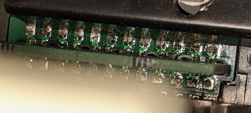
Figure 7. Unfortunately, there is a problem. A restraining device like this metal bracket may impinge on the exposed solder joints that attach the individual header pin sockets to the horizontal circuit board. If the device is conductive or if it has a non-conductive coating that can wear away, these pins may be shorted. The designs of modern pin header sockets and of the original IBM plug connector make it unlikely that a different circuit board design can avoid this issue.
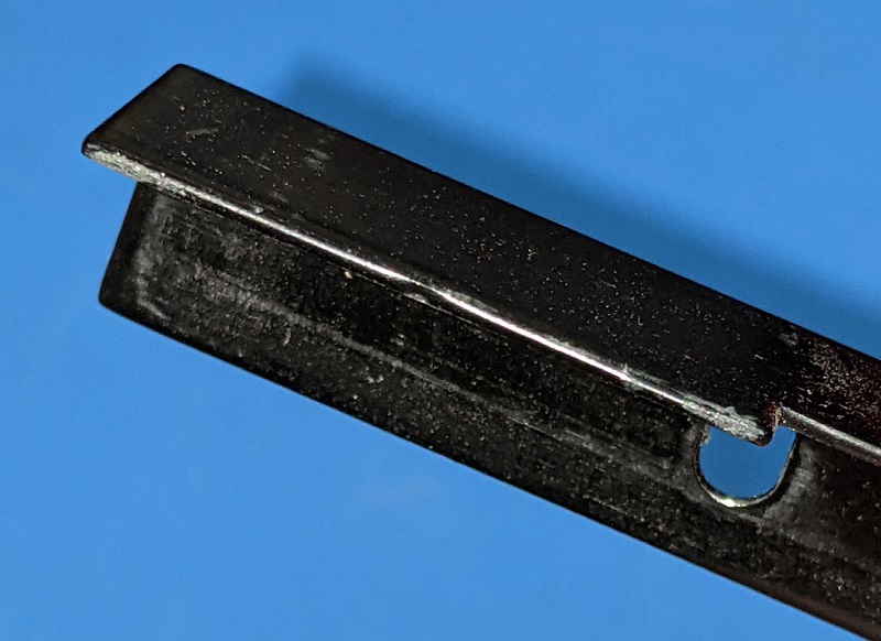
Figure 8. This close-up of the IBM 5100's bracket suggests that its enamel coating is already wearing away. The best option for avoiding shorts in situations like these may be to add additional layers of insulation between the adaptor and the restraint. One specific option in this setting could be to apply a durable lacquer or varnish to the solder joints, and then to supplement the bracket's enamel coating with a folded strip of polyimide ("Kapton") tape.
Our adaptors require shorter "low profile" components in order to fit in the same places where the original IBM plugs and sockets were designed to go.
For socket adaptors, the header pin sockets should extend no further than 5.2mm from the horizontal circuit board. So far, the components used have been Samtec CES-101-01-S-S single-pin sockets, though socket adaptors made with these may be more liable to "back out" from original IBM plugs than the IBM sockets were. Note that using even shorter pin-header sockets than these might cause the adaptor to rest too low in the plug for the original restraint to keep it in place.
For plug adaptors, the header pins should probably not have a mating contact length that extends beyond 5mm. So far, the components used have been single-pin 3M 951101-8622-AR pins (no convenient link).
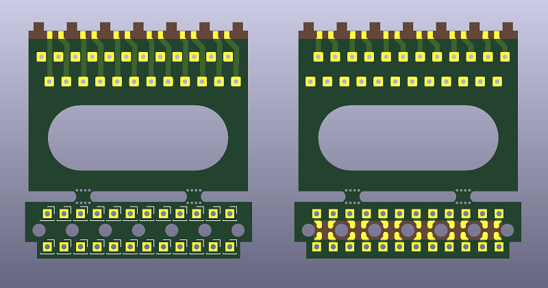
The design files in this repository describe a single "combined" circuit board with two detachable pieces. The image above shows both sides of this combined board. Its lower detachable portion forms the "horizontal" circuit board while the upper portion forms the "vertical" circuit board.
Both sides of the vertical circuit board are functionally identical. The horizontal circuit board is different: it has one side with bare metal "fingers" that reach in towards its centre (bottom right in the image).
Detach the vertical and horizontal circuit boards and the two small connecting stubs across all perforations. Throw the stubs away. Using sandpaper, a file, an emery board, or some other abrasive tool, file down any remnants of the stub that protrude from the edges of the circuit boards.
Plug the tabs of the vertical circuit board into the holes in the horizontal circuit board, making certain that the bare fingers on the horizontal circuit board are next to the exposed metal traces on the vertical circuit board. Trace the connections from the horizontal board pins/sockets to the vertical board plated through holes to make sure the arrangement suits your needs; if not, flip the vertical board over.
Temporarily secure both boards so that they are as close to perpendicular as possible, then solder the vertical board to the horizontal board by making angled solder bridges between each horizontal board finger and its nearest vertical board exposed trace.
Install pin-header pins or sockets so that they extend from the horizontal board on the side opposite the vertical board. This is the trickiest part of assembly as both pins and sockets can wiggle around a lot. It may be marginally easier if you are assembling one plug adaptor and one socket adaptor simultaneously. Try plugging your pins and sockets into each other, then sandwiching them between two horizontal boards to create an arrangement similar to figure 5 above. Naturally you will want all of the pins to be attached to one horizontal board and all of the sockets to be attached to the other.
You will need to pinch both connectors together until you have a few of the pins and sockets tacked into place with solder. From there, as you solder the rest of the pins and sockets in place, it may be useful to use a pair of tweezers to rotate and reposition the pin/socket pairs so that they are lined up as neatly as possible.
Tidy the pins and sockets. Reflowing each pin or socket solder joint and manually aligning the pins or sockets can help arrange them even more neatly. An additional tactic available to people making a plug adaptor and a socket adaptor at the same time is to plug the adaptors into each other with various misalignments and offsets, then reflow mated pin and socket joints individually in hopes that pins and sockets will change position slightly to accommodate the positions of their nonstandard counterparts. With a few iterations of this a more regular average positioning might be achieved, but your mileage may vary.
To the fullest extent possible, this design is released into the public domain. Nobody owns it.
Thanks as usual are owed to the bitsavers.org archive of technical documentation.
22 August 2021: Initial release (Tom Stepleton, stepleton@gmail.com, London)
| Qty | Value | Footprint | References |
|---|---|---|---|
| 24 | Conn_01x01 | Connector_Wire:SolderWire-0.25sqmm_1x01_D0.65mm_OD1.7mm | J101, J102, J103, J104, J105, J106, J107, J108, J109, J110, J111, J112, J113, J114, J115, J116 +8 |
| 24 | Conn_01x01_Female | Connector_PinSocket_2.54mm:PinSocket_1x01_P2.54mm_Vertical | J1, J2, J10, J11, J12, J13, J14, J15, J16, J17, J18, J19, J20, J21, J22, J23 +8 |
The 48 most common of 57 parts.
It measures 43.5 × 45.3 mm and has 2 copper layers, 1.6 mm thick.
57 parts. The full list of its parts is on this page, with links to each part's symbol and footprint where PCBKit's library has them.
From the stepleton/SLT_interconnect repository on GitHub, at the commit this page was made from: the board is SLT_interconnect.kicad_pcb. PCBKit opens the board in the browser, with nothing to install.
Its repository publishes it under the Unlicense licence: you may reuse it on that licence's terms (keep the author's notice, and for a copyleft licence share your changes alike).


tapioki/cephalopoda
Low profile split ergonomic mechanical keyboards

rgoulter/keyboard-labs
Repo with my PCB designs and keyboard firmware

freeDSP/freeDSP-aurora
freeDSP ADAU1452 with 8 analog input, 8 analog outputs, S/P-DIF I/O, ADAT I/O, USB Audio Class2, WiFi, Bluetooth
