
4 layers34 × 34 mm
BSN N54
Stachu1/BLE_Sensor_Node
KiCad project: BSN-N54.kicadpro. See the root README for the board naming scheme.
46 parts
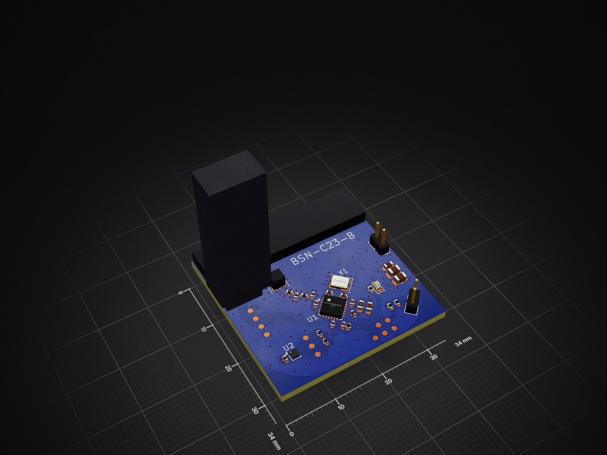
 Stachu1/BLE_Sensor_Node
KiCad project: BSN-N54.kicadpro. See the root README for the board naming scheme.
BSN C23 is an open-source printed circuit board by Stachu1, from the Stachu1/BLE_Sensor_Node repository on GitHub. It is a 4-layer board of 34 × 34 mm with 47 parts on 28 nets, routed with 192 tracks and 156 vias.
It is built around the MM8130-2600RA2. Its parts include 15 capacitors, 6 resistors, 4 connectors, 4 inductors and 2 ICs.
Concluded at rev A. The N54 was compared with the C23 on rev A, and rev B uses the CC2340R5. See
MCU_DECISION.md. This folder is kept as the record of that comparison.
KiCad project: BSN-N54.kicad_pro. See the root README for the board naming scheme.
BSN-N54-A)Ordered as a separate design from BSN-C23-A (not panelized). Firmware, bring-up procedure and per-board
results: firmware/N54 and firmware/N54/BRINGUP.md.
| Board | BLE address | Status |
|---|---|---|
| #1 | EC:A6:80:CE:7A:1A | Full build except U2 (SHTC3) and X2 (32 kHz). hwtest 13/13 PASS. ble_sensor advertises BTHome and is decoded with tools/bsn_scan.py. Antenna side fitted with the C23 values (L6 4.3 nH, 2.1 pF shunt), not verified on this layout (see below). PA network as designed, which loses about 10 dB (see board #2). |
| #2 | FA:28:B5:E0:85:F5 | MCU + U.FL, no antenna, no U2/X2. hwtest 13/13 PASS. A*: PA network bypassed. Used for the crystal trim, conducted power and the current measurements. |
testing/RF/RF_CARRIER.md. HFXO trim 11.75 pF (+127 ppm at the datasheet
7 pF). The reference PA network as laid out costs 10–11 dB. Bypassed, the PA gives 0.0 dBm at the 0 dBm
setting and +7.5 dBm at +8 dBm.testing/Power/POWER_MEASUREMENTS.md. Floor 4.20 µA
(System OFF 2.05 µA, both about 1.4 µA above the datasheet on both boards, cause not found), 7.6 µC per advert
at 0 dBm, 2.01 / 1.78 µC per sensor reading with timer / DRDY wake (C23: 0.366 µA, 12.6 µC, 9.56 / 3.72 µC).Hand-modified boards are marked A* (see the root README).
| Board | Date | Change | Reason |
|---|---|---|---|
| #1 | 2026-10-27 | Antenna side: 4.3 nH series and 2.1 pF shunt (the C23 match) | Same antenna as C23. Not re-matched: AE1 is fed from the other end than on C23 (rotated 180°, feed pad at x = 146.75 instead of 153.25) through a longer trace, so the match is only a starting point |
| #2 | 2026-10-27 | X1 reflowed | Checking the +127 ppm offset (no change) |
| #2 | 2026-10-27 | PA network bypassed: 15 pF in series at L2 (DC block), L3 and L4 bridged, C14, C15, C16 removed. R4 0 Ω and J1 kept | The network cost 10–11 dB. Bypassed, the output matches the datasheet |
| #2 | 2026-10-27 | Cleaned with IPA | Checking whether flux explains the high floor current (no change) |
The antenna matching network on the nRF54L05 ANT pin (U1 pin 31) is the Nordic reference PA network (nRF54L datasheet, circuit configuration 1 for QFN48: L2, C14, L3, C15, L4, C16), followed by the antenna match (L5, L6, L7) and the U.FL test point (R4, J1).
U1.ANT(31) ─ L2 ─┬─ L3 ─┬─ L4 ─┬──────────── L6 ─┬─ AE1
               C14    C15    C16   L5      │     L7
                │      │      │    │      R4     │
              VSS_PA  GND    GND  GND      │    GND
(pin 32) J1| Ref | Value | Role |
|---|---|---|
| L2, C14, L3, C15, L4, C16 | 2.7 nH, 1.5 pF, 3.5 nH, 2.0 pF, 3.5 nH, 0.3 pF | Nordic reference PA network (0201 in the reference, 0402 here) |
| L5 | 7.3 nH | Shunt to GND on the J1 node (antenna side) |
| L6 | 6.7 nH | Series to the antenna |
| L7 | Shunt at the antenna feed | |
| R4, J1 | 0 Ω, U.FL | Test point, not fitted in normal use |
C14 grounds only to pin 32 (VSS_PA), which only joins the centre pad, and C15 grounds straight to the bottom plane with no inner-layer fill, as Nordic's notes require.
Measured on rev A: this network, as laid out with 0402 parts, cost 10–11 dB into 50 Ω (see
testing/RF/RF_CARRIER.md). A rev B N54 should copy Nordic's 0201 layout exactly and
verify the PA network into 50 Ω on its own before the antenna is matched.
Before the boards existed, the MCU source impedance and the antenna impedance were estimated from the nRF54L and
antenna datasheets and stepped through all 8 elements on a Smith chart. This treated L5 as a series part, which it
isn't on the board, and the estimated antenna impedance was later measured on C23 to be quite different
(about 6.4 − j13 Ω, see hardware/C23/testing/rev_A/RF/ANTENNA_MATCHING.md). Kept for reference:
A simplified 3-element equivalent from the same estimate:
| Qty | Value | Footprint | References |
|---|---|---|---|
| 12 | TestPoint | TestPoint:TestPoint_Pad_D1.0mm | TP1, TP2, TP3, TP4, TP5, TP6, TP7, TP8, TP9, TP10, TP11, TP12 |
| 7 | 100n | Capacitor_SMD:C_0402_1005Metric | C2, C3, C4, C11, C12, C14, C15 |
| 2 | 1.5p | Capacitor_SMD:C_0402_1005Metric | C8, C9 |
| 2 | 100k | Resistor_SMD:R_0402_1005Metric | R3, R4 |
| 2 | 100u | Capacitor_SMD:C_0805_2012Metric | C5, C6 |
| 2 | 10u | Capacitor_SMD:C_0603_1608Metric | C1, C10 |
| 2 | 4.7k | Resistor_SMD:R_0402_1005Metric | R5, R6 |
| 2 | Conn_01x02 | Connector_PinHeader_2.00mm:PinHeader_1x02_P2.00mm_Vertical | J1, J4 |
| 1 | 0R | Resistor_SMD:R_0402_1005Metric | R1 |
| 1 | 1.6n | Inductor_SMD:L_0402_1005Metric | L2 |
| 1 | 10u | Inductor_SMD:L_0603_1608Metric | L4 |
| 1 | 15p | Capacitor_SMD:C_0402_1005Metric | C7 |
| 1 | 1k | Resistor_SMD:R_0402_1005Metric | R2 |
| 1 | 1u | Capacitor_SMD:C_0402_1005Metric | C13 |
| 1 | 2.8n | Inductor_SMD:L_0402_1005Metric | L1 |
| 1 | 48MHz | Crystal:Crystal_SMD_3225-4Pin_3.2x2.5mm | X1 |
| 1 | 6.8n | Inductor_SMD:L_0402_1005Metric | L3 |
| 1 | CC2340R52E0RGER | BSN-C23:Texas_RGE0024B_VQFN-24-1EP_4x4mm_P0.5mm_EP2.45x2.45mm_ThermalVias | U1 |
| 1 | CR2032_Holder | Battery:BatteryHolder_Renata_SMTU2032-LF_1x2032 | BT1 |
| 1 | Conn_ARM_SWD_TagConnect_TC2030-NL | Connector:Tag-Connect_TC2030-IDC-NL_2x03_P1.27mm_Vertical | J3 |
| 1 | HDC2010 | BSN-C23:HDC2010 | U2 |
| 1 | IFA_2G4 | BSN-C23:IFA_2G4 | AE1 |
| 1 | LED | LED_SMD:LED_0603_1608Metric | D1 |
| 1 | MM8130-2600RA2 | BSN-C23:Murata_MM8130-2600 | J2 |
It measures 34 × 34 mm and has 4 copper layers, 1.61 mm thick.
47 parts, built around the MM8130-2600RA2. The full list of its parts is on this page, with links to each part's symbol and footprint where PCBKit's library has them.
From the Stachu1/BLE_Sensor_Node repository on GitHub, at the commit this page was made from: the board is hardware/C23/BSN-C23.kicad_pcb and its schematic hardware/C23/BSN-C23.kicad_sch. PCBKit opens the board in the browser, with nothing to install.
Its repository states no licence, so its author keeps all rights: ask Stachu1 before reusing the design.
Stachu1/BLE_Sensor_Node
KiCad project: BSN-N54.kicadpro. See the root README for the board naming scheme.

antmicro/m2-smart-iot-module
https://antmicro.com/blog/2021/08/open-hardware-smart-m2-radio-module-for-iot/


332753-art/Water_Quality_Monitoring
portable Water Quality Monitoring System for Live Fish Transport

ephrenm/VehiCell
NRF9151-based cellular telemetry device designed for a FSAE EV vehicle.


EPFLXplore/XRE_LeggedRobot_HW
PCB designs for Xplore Research's robot dog project
