


2 layers60 × 111.3 mm
Silkscreen pcb
iandchasse/silkscreen-pcb
Silkscreen: open-hardware ESP32-S3 e-paper reader mainboard (KiCad 9). Formerly the de-link hub.
189 parts589CERN-OHL-S-2.0
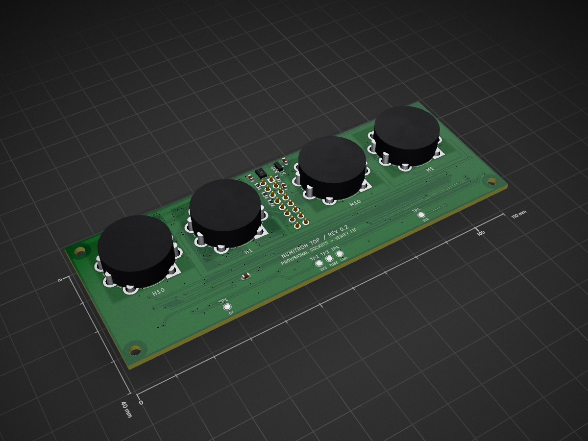
 spott/NumitronClock
Four-tube RCA DR2000 Numitron desk clock: KiCad top board, docs and datasheets
NumitronTop is an open-source printed circuit board by spott, from the spott/NumitronClock repository on GitHub. It is a 2-layer board of 110 × 40 mm with 59 parts on 69 nets, routed with 1,176 tracks and 184 vias.
It is built around the BH1750FVI-TR, RC0603FR-07100KL and RC0603FR-071KL, with the RC0603FR-0710KL among its other parts. Its parts include 21 resistors, 15 capacitors, 8 ICs, 1 transistor and 1 connector. It belongs with the lEDs and displays boards of this library.
Top-board schematic and PCB layout for the four-tube clock described in the Obsidian note electronics/Numitron Clock/Numitron Clock.md, read on 2026-09-18. The detailed top-board decisions in that note supersede its older, general power and interconnect descriptions.
Open NumitronTop.kicad_pro in KiCad. The design was captured and checked with KiCad 10.0.5. All schematic symbols are included in the project-local library and embedded in the sheets.
The top board is placed and routed on a 110 × 40 mm working outline with all 55 schematic parts, four M2.5 mounting positions, local power distribution and ground copper on both faces. The extra depth provides a separate underside strip for the wide SOIC drivers. The layout notes explain component placement, the perpendicular underside connector orientation and review process.
The GZC9-A socket footprint remains provisional, as explicitly authorized on 2026-09-25: 18 mm assumed tail circle, 0.5 mm estimated terminal thickness, 2.5 mm plated holes and 3.8 mm copper lands. Verify physical fit before ordering. Enclosure/cable fit, exact capacitor order codes and hardware measurements also remain assembly/release checks. WWVB versus GPS belongs to the bottom board.
The owner confirms the actual tubes are marked DR2000 and have prefix decimal points. The archived RCA table assigns that feature to DR2010 instead. The design preserves the requested HH.MM display and routes the eighth channel to pin 1; verify that decimal connection on the actual tubes before enabling it.
The reusable async ES100 driver and Pico 2 breadboard program live in
firmware/. Build and check them with the pinned firmware
toolchain (Rust/Cargo, Pico 2 target, flip-link and picotool are supplied by Nix):
nix develop .#firmware --command bash scripts/check_firmware.shThe generated UF2 is firmware/target/pico2-es100.uf2. See the firmware guide for
wiring, BOOTSEL flashing, USB logs and the hardware test handoff. Physical
reception has not been validated; this does not decide WWVB versus GPS.
Use the pinned Nix flake; no global package installation is required. KiCad is supplied by the existing local application installation on macOS. The flake pins the supporting Python, Poppler, SVG-rendering and local Freerouting tools, not that external KiCad application.
nix develop
bash scripts/review.sh
The review command runs KiCad ERC, audits the saved schematic's netlist and provisional socket footprint, exports schematic and footprint SVGs, and renders inspection PNGs under ignored tmp/render/. It does not regenerate or overwrite the schematic or footprint. Source PDFs and the socket drawing are archived in Git with their provenance and hashes.
scripts/build_schematic.py --write records the initial schematic capture and is deliberately opt-in: it overwrites the native KiCad files. After editing in KiCad, preserve those edits; reconcile the generator before using it again.
hardware/top-board/socket-footprint.json records the socket assumptions. scripts/build_socket_footprint.py --write captures them into the project-local Numitron.pretty library; reconcile manual footprint edits before regenerating. The schematic assigns Numitron:GZC9-A_B9A_Provisional to V1-V4.
nix develop --command bash scripts/review_placement.sh checks the saved PCB against the netlist, runs DRC with schematic parity and generates the top/bottom review drawings. It does not regenerate placement or routing. board-drc.json and placement-checks.txt retain the results.
build_placement.py --write is a one-time placement capture using KiCad's bundled Python; it refuses to discard routing without an explicit override. placement.json is the initial coordinate record, while the saved native board is authoritative. The power routing, local-router exchange and ground-fill helpers likewise require care around later CAD edits; do not run capture scripts just to review the design.
The repository covers the future whole clock. Its hardware design currently contains only the top board; the Pico 2 firmware is a separate time-receiver experiment. The bottom board will supply protected 5 V, regulated 3.3 V, the control interface and I2C pull-ups. Its schematic and layout remain future work.
| Qty | Value | Footprint | References |
|---|---|---|---|
| 8 | 100n 50V X7R | Capacitor_SMD:C_0603_1608Metric | C4, C5, C6, C7, C8, C10, C12, C14 |
| 7 | 4.7k | Resistor_SMD:R_0603_1608Metric | R11, R12, R13, R14, R17, R20, R21 |
| 4 | 1u 25V X7R | Capacitor_SMD:C_0805_2012Metric | C9, C11, C13, C15 |
| 4 | 33R | Resistor_SMD:R_0603_1608Metric | R3, R4, R5, R6 |
| 4 | DR2000 / GZC9-A | Numitron:GZC9-A_B9A_Provisional | V1, V2, V3, V4 |
| 4 | M2.5 / NPTH 2.7 | Numitron:MountingHole_2.7mm_M2.5_BothSides | H1, H2, H3, H4 |
| 4 | TPIC6B595DWR | Package_SO:SOIC-20W_7.5x12.8mm_P1.27mm | U5, U6, U7, U8 |
| 3 | 100k | Resistor_SMD:R_0603_1608Metric | R7, R8, R9 |
| 3 | 10u 25V X7R | Capacitor_SMD:C_1206_3216Metric | C1, C2, C3 |
| 2 | 1k | Resistor_SMD:R_0603_1608Metric | R15, R18 |
| 2 | 2.2k | Resistor_SMD:R_0603_1608Metric | R10, R16 |
| 1 | +3V3 | TestPoint:TestPoint_Pad_D1.5mm | TP2 |
| 1 | +5V | TestPoint:TestPoint_Pad_D1.5mm | TP1 |
| 1 | 10k | Resistor_SMD:R_0603_1608Metric | R19 |
| 1 | 10k 1% | Resistor_SMD:R_0603_1608Metric | R2 |
| 1 | 46.4k 1% | Resistor_SMD:R_0603_1608Metric | R1 |
| 1 | 61201621621 | Numitron:Wurth_61201621621_2x08_P2.54mm | J1 |
| 1 | AP7361C-Y5-13 | Numitron:Diodes_SOT89-5_AP7361C | U1 |
| 1 | BH1750FVI-TR | Numitron:ROHM_WSOF6I_BH1750_NoCenterPad | U3 |
| 1 | GND | TestPoint:TestPoint_Pad_D1.5mm | TP4 |
| 1 | MMBT3904-7-F | Package_TO_SOT_SMD:SOT-23 | Q1 |
| 1 | SER_OUT 5V | TestPoint:TestPoint_Pad_D1.5mm | TP5 |
| 1 | SN74AHCT125DR | Package_SO:SOIC-14_3.9x8.7mm_P1.27mm | U2 |
| 1 | TLV809EA29DBZR | Package_TO_SOT_SMD:SOT-23 | U4 |
| 1 | V_TUBE | TestPoint:TestPoint_Pad_D1.5mm | TP3 |
It measures 110 × 40 mm and has 2 copper layers, 1.6 mm thick.
59 parts, built around the BH1750FVI-TR, RC0603FR-07100KL, RC0603FR-071KL and RC0603FR-0710KL. The full list of its parts is on this page, with links to each part's symbol and footprint where PCBKit's library has them.
From the spott/NumitronClock repository on GitHub, at the commit this page was made from: the board is hardware/top-board/NumitronTop.kicad_pcb and its schematic hardware/top-board/ControlAndSensor.kicad_sch. PCBKit opens the board in the browser, with nothing to install.
Its repository states no licence, so its author keeps all rights: ask spott before reusing the design.
iandchasse/silkscreen-pcb
Silkscreen: open-hardware ESP32-S3 e-paper reader mainboard (KiCad 9). Formerly the de-link hub.


EwoudVV/ducktop2
An open-source 16-inch laptop designed from scratch.


magnus188/aegir
Open-source ESP32-P4 trimix analyzer prototype for technical diving,

benkrasnow/1v2-boost-converter
Schematics and PCB layout for a boost converter 0.9V minimum input, 30A maximum input current

jonahsaunders/planar-studio
KiCad extension for the copper you can't buy as a part — design planar inductors, transformers, PCB motor stators, filters, and antennas, with electrical modeling and direct write-back to your board.

nuerolynx/embedded-systems-lab
Arduino UNO R4 WiFi and ESP32 prototypes for access control, automation, displays, monitoring, and Bluetooth audio.