
4 layers99 × 53.3 mm
PSLab
fossasia/pslab-hardware
PSLab Hardware Design and Schematics https://pslab.io
199 parts1.7kApache-2.0

 sp7q/HS-LDZ_badge1
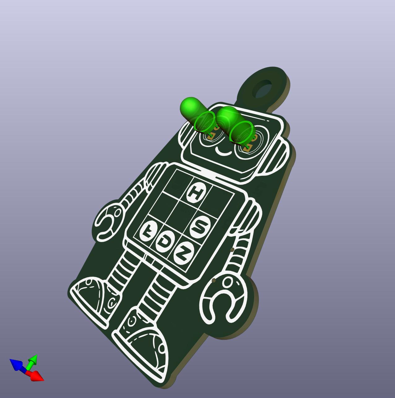
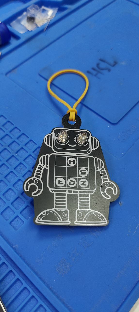
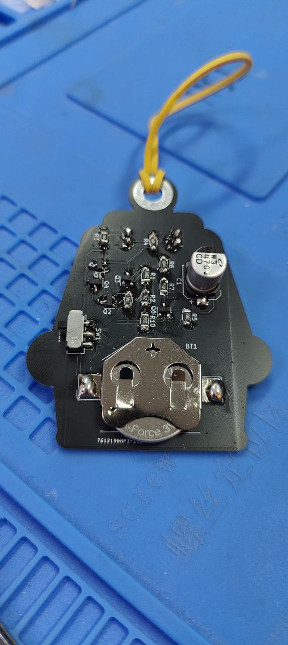
Hakierspejs Łódź badge, on which we teach people how to solder.
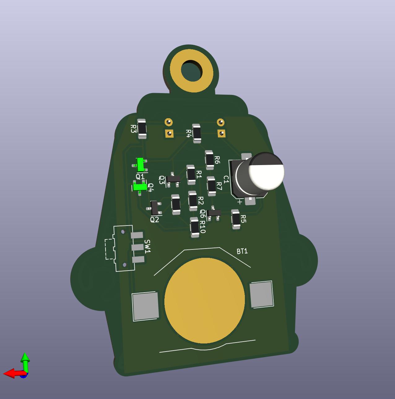
HS badge is an open-source printed circuit board by sp7q, from the sp7q/HS-LDZ_badge repository on GitHub. It is a 2-layer board of 54.9 × 69.9 mm with 21 parts on 13 nets, routed with 90 tracks and 0 vias.
It is built around the MMBT3904 and MMBT3906. Its parts include 9 resistors, 5 transistors, 2 diodes, 1 capacitor and 1 switch. It belongs with the lEDs and displays boards of this library.
Hakierspejs Łódź badge, on which we teach people how to solder.
Simple circuit
Small number of components
Relatively short assembly time
Practical use
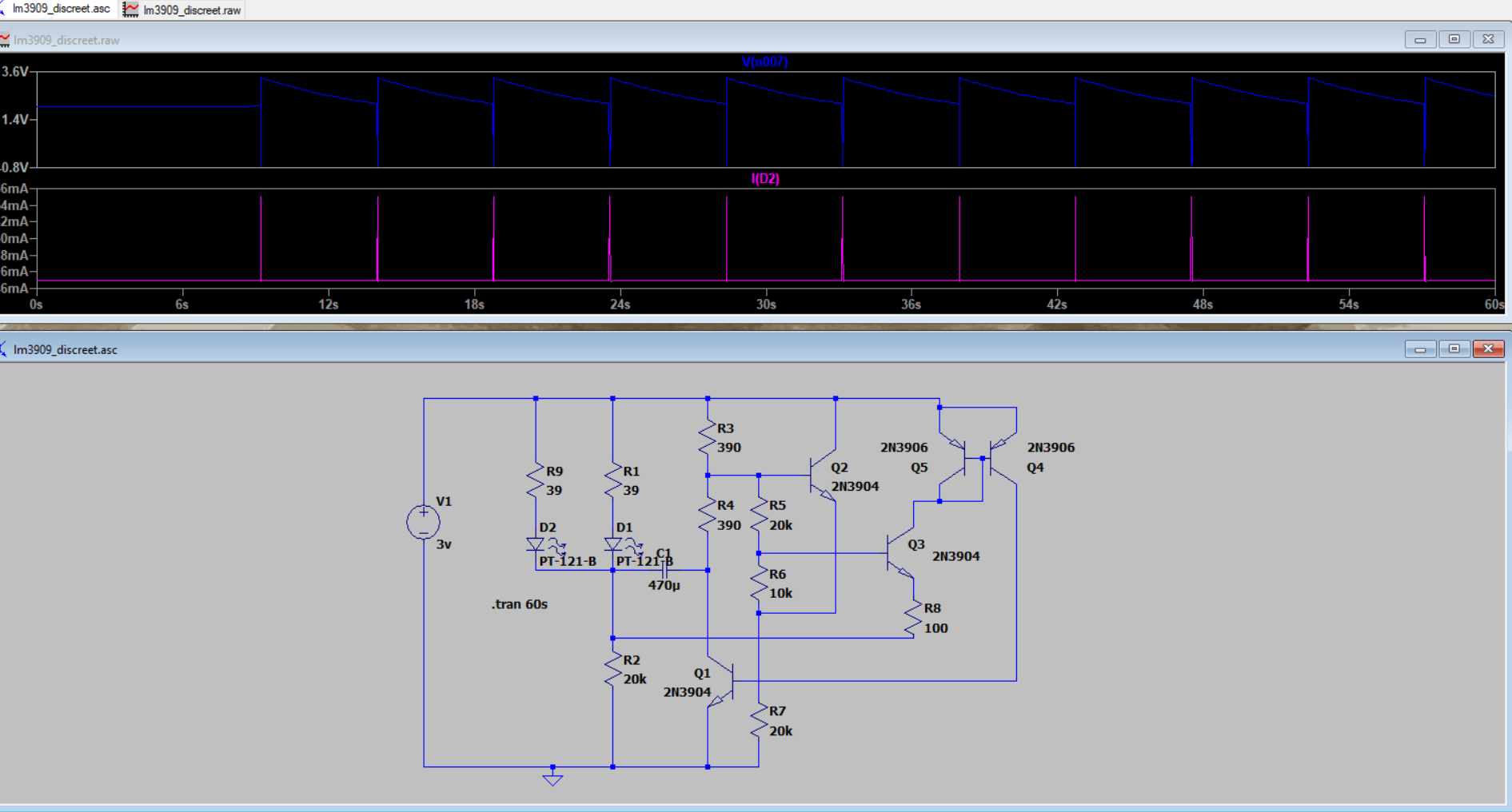
The circuit is an implementation of the LM3909 using discrete components, based on the design from the link below :
(https://www.righto.com/2021/01/reverse-engineering-low-power-led.html)
LTspice model is based on work from link :
(https://softsolder.com/2020/09/03/discrete-transistor-lm3909-led-flasher/)
| Qty | Value | Footprint | References |
|---|---|---|---|
| 3 | 100 | Resistor_SMD:R_1206_3216Metric_Pad1.30x1.75mm_HandSolder | R3, R4, R8 |
| 3 | 20k | Resistor_SMD:R_1206_3216Metric_Pad1.30x1.75mm_HandSolder | R1, R5, R10 |
| 3 | MMBT3904 | Package_TO_SOT_SMD:TSOT-23_HandSoldering | Q2, Q3, Q6 |
| 2 | 390 | Resistor_SMD:R_1206_3216Metric_Pad1.30x1.75mm_HandSolder | R6, R7 |
| 2 | LED | LED_THT:LED_D5.0mm | D1, D2 |
| 2 | MMBT3906 | Package_TO_SOT_SMD:TSOT-23_HandSoldering | Q1, Q4 |
| 1 | 10k | Resistor_SMD:R_1206_3216Metric_Pad1.30x1.75mm_HandSolder | R2 |
| 1 | 200u | Capacitor_SMD:CP_Elec_8x10.5 | C1 |
| 1 | Battery_Cell | Battery:BatteryHolder_Keystone_3002_1x2032 | BT1 |
| 1 | LOGO | cat:robot1_60_eye | |
| 1 | SW_SPST | Button_Switch_SMD:SW_SPDT_CK-JS102011SAQN | SW1 |
The 20 most common of 21 parts.
fossasia/pslab-hardware
PSLab Hardware Design and Schematics https://pslab.io

AndersBNielsen/Relatively-Universal-ROM-Programmer
Hardware to program W27C512 EEPROM or any 24/28/32 pin ROM requiring from 5V to 27V programming voltage.


mzuelch/CATs-Eurosynth
Analog Synth Eurorack Modules


ThisIsNotRocketScience/Eurorack-Modules
This is not Rocket Science presents: Eurorack modular synthesizer modules!

It measures 54.9 × 69.9 mm and has 2 copper layers, 1.6 mm thick.
21 parts, built around the MMBT3904 and MMBT3906. The full list of its parts is on this page, with links to each part's symbol and footprint where PCBKit's library has them.
From the sp7q/HS-LDZ_badge repository on GitHub, at the commit this page was made from: the board is KiCAD files/HS badge.kicad_pcb and its schematic KiCAD files/HS badge.kicad_sch. PCBKit opens the board in the browser, with nothing to install.
Its repository states no licence, so its author keeps all rights: ask sp7q before reusing the design.