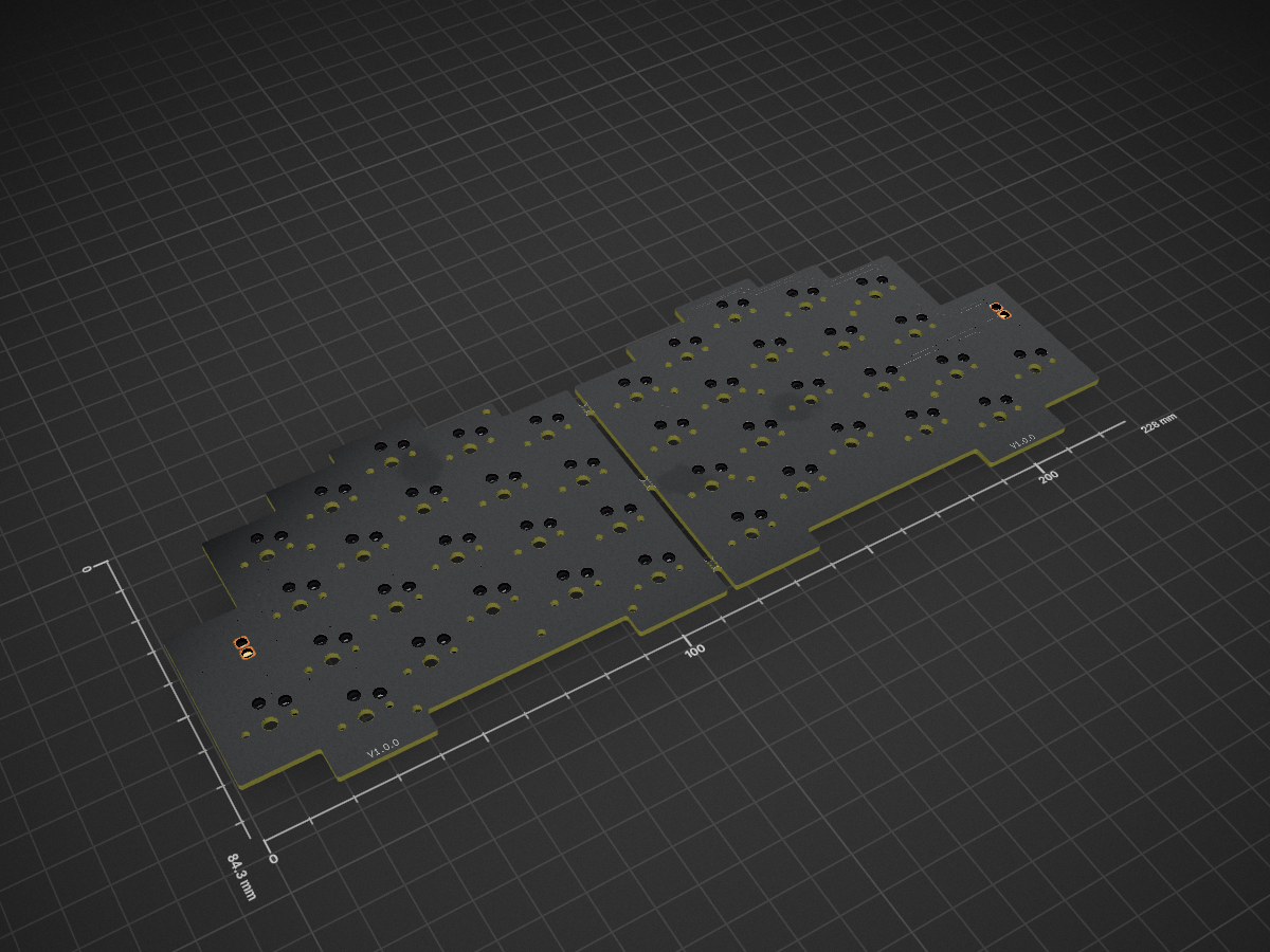
2 layers247.9 × 104.5 mm
 Soham1101/Split-Keyboard
Title: Setting up KiCad project and installing all libraries Started the split keyboard project today. The first challenge was just getting the environment set up correctly turns out this project needs a bunch of…
Soham PCB NoErrors is an open-source printed circuit board by Soham1101, from the Soham1101/Split-Keyboard repository on GitHub. It is a 2-layer board of 228 × 84.3 mm with 107 parts on 83 nets, routed with 652 tracks and 31 vias.
Its parts include 42 diodes, 42 switches, 4 resistors and 2 ICs. It belongs with the nRF52 and nRF5x boards of this library.
Journal entries:
Entry 1:
Title: Setting up KiCad project and installing all libraries Started the split keyboard project today. The first challenge was just getting the environment set up correctly turns out this project needs a bunch of external libraries that don't come with KiCad by default, and hunting them all down took longer than expected.
Created a fresh KiCad project and immediately hit issues with missing footprint libraries. The first thing I had to track down was the Seeed Studio XIAO Series Library this contains the schematic symbol for the XIAO nRF52840, which is the brain of this keyboard. I downloaded it from their OPL GitHub repo and added it via Preferences → Manage Symbol Libraries.
Then came marbastlib from ebastler on GitHub this has all the Kailh Choc v1 hotswap socket footprints I need for the switches. Installation was a bit fiddly because it needs to be added as a project-level footprint library, not a global one.
After that, Panelization.pretty for the mousebite/breakoff footprints. These are the little perforated connections that will hold the two halves of the keyboard together during manufacturing so they ship as one PCB.
The most important one was the custom XIAO nRF52840 footprint a modified version of the official Seeed foot print that exposes the battery charging pins on the bottom of the board. Without this, you can't connect a LiPo battery. Dropped the .kicad_mod file into my project folder and added it as a local library.
Once all libraries were in place, I set up the hierarchical sheet structure in the schematic editor. This is the clever trick that makes split keyboards easy to design: create two sheet references in the root schematic, both pointing to the same side.kicad_sch file one named "left" and one named "right". Changes to one side automatically reflect on the other.
Entry 2: Title: Designing the keyboard matrix schematic Today was the bulk of the schematic work. Spent most of the session inside side.kicad_sch building out the keyboard matrix this is the circuit that both halves will share.
Understanding the matrix: The XIAO nRF52840 doesn't have enough GPIO pins to wire every key directly (21 keys per half would need 21 pins). The keyboard matrix solves this by arranging switches in a grid of rows and columns. With 5 columns and 5 rows (plus 1 thumb row), I only need 10 pins total instead of 21. The firmware scans each column one at a time and reads which row lines go high to detect keypresses.
I chose diodes because every switch needs its own diode to prevent "ghosting" a bug where pressing multiple keys at once causes the controller to detect phantom keypresses due to current flowing backwards through the matrix. Each diode only allows current in one direction, isolating each switch. I used SOD-123 SMD diodes (1N5819 style) since they're compact and can sit right next to each switch on the PCB.
Placed the XIAO nRF52840 symbol and built the 5×5 matrix plus 1 thumb key row. Each switch+diode unit connects its switch to the column net and diode cathode to the row net. Used KiCad net labels (L shortcut) like COL0–COL4 and ROW0–ROW4 to keep the schematic clean instead of routing long wires everywhere.
Connecting the labels to the XIAO pins: Columns to pins P0.02, P0.03, P0.28, P0.29, P0.04 Rows to pins P1.15, P1.14, P1.13, P1.12, P1.11
Battery circuit: The XIAO has battery management built in just needed two test point pads (one VBAT, one GND) connected to the BAT pin. Also added the optional battery voltage divider: VBAT -> 806kΩ resistor -> BT_PIN node -> 2MΩ resistor -> GND The BT_PIN connects to an analog pin on the XIAO (P0.02/A0) so ZMK firmware can report battery percentage over Bluetooth.
Mounting holes: Added 5x M2 mounting holes in the schematic. These will become physical standoff mounting points on the PCB for attaching a case or just for stability.
Ran ERC (Tools → Electrical Rules Checker) at the end had 2 warnings about unconnected pins (the NFC pins on the XIAO which we're not using), resolved them with no-connect flags.
Entry 3: Title: Assigning footprints and starting PCB layout Footprint assignment: Opened Tools and Assign Footprints and went through every component:
XIAO nRF52840 → local-footprints:modified-XIAO-nRF52840-SMD (the custom one) Switches (x21 per half) → PCM_marbastlib-choc:SW_choc_v1_HS_CPG135001S30_1u Diodes → Diode_SMD:D_SOD-123 Resistors → Resistor_SMD:R_0805_2012Metric Battery test points → TestPoint:TestPoint_Pad_D2.0mm Mousebites → panelization:mouse-bite-2mm-slot Mounting holes → MountingHole:MountingHole_2mm Went with Kailh Choc v1 hotswap sockets because they're low-profile and the hotswap means I can swap switches later without desoldering important since I'm not sure which switches I'll prefer yet.
Opening the PCB editor: After updating the PCB from schematic (Tools → Update PCB from Schematic), all 84 footprints appeared as a giant rats nest pile in the middle of the board. The rats nest lines (thin airwires showing unrouted connections) make it look like spaghetti at this point.
Layout strategy: For a split keyboard, each half is basically identical but mirrored. So the plan is:
Layout one half completely Draw the edge cuts (board outline) for that half Mirror it horizontally to create the other half Position both halves next to each other with a small gap for the mousebites Started placing the left half. Put the XIAO at the top-left, switches arranged in the 5×5 matrix grid pattern matching the schematic layout. The Choc v1 sockets have a specific footprint with the switch cutout and two hotswap pads need to make sure they're all oriented correctly (the switch orientation matters for the keycap legends).
Diodes placed directly below each switch socket, oriented with cathode pointing down toward the row line. This keeps each switch+diode pair tight and the routing short.
Ran into a courtyard overlap issue with a few components that were too close nudged them slightly apart and it cleared up.
| Qty | Value | Footprint | References |
|---|---|---|---|
| 42 | 1N5819 | Diode_SMD:D_SOD-123 | D2, D3, D4, D10, D11, D12, D13, D14, D15, D16, D17, D18, D19, D20, D21, D22 +26 |
| 42 | SW_Push | PCM_marbastlib-choc:SW_choc_v1_HS_CPG135001S30_1u | SW10, SW11, SW12, SW13, SW14, SW15, SW16, SW17, SW18, SW19, SW20, SW21, SW22, SW23, SW26, SW27 +26 |
| 10 | MountingHole | MountingHole:MountingHole_2mm | H1, H2, H3, H4, H5, H6, H7, H8, H9, H10 |
| 3 | break off | panelization:mouse-bite-2mm-slot | BO1, BO2, BO3 |
| 2 | 2M | Resistor_SMD:R_0805_2012Metric | R3, R10 |
| 2 | 806k | Resistor_SMD:R_0805_2012Metric | R2, R9 |
| 2 | BAT | TestPoint:TestPoint_Pad_D2.0mm | TP1, TP2 |
| 2 | GND | TestPoint:TestPoint_Pad_D2.0mm | TP4, TP8 |
| 2 | XIAO-nRF52840-SMD | mito-simplified:XIAO-nRF52840-SMD | U1, U3 |
It measures 228 × 84.3 mm and has 2 copper layers, 1.61 mm thick.
107 parts. The full list of its parts is on this page, with links to each part's symbol and footprint where PCBKit's library has them.
From the Soham1101/Split-Keyboard repository on GitHub, at the commit this page was made from: the board is soham-PCB-NoErrors.kicad_pcb and its schematic side.kicad_sch. PCBKit opens the board in the browser, with nothing to install.
Its repository states no licence, so its author keeps all rights: ask Soham1101 before reusing the design.


zueblin/Polaron
A DIY drum machine for the teensy microcontroller (hardware / software)


ChrisChrisLoLo/pusheenz40
A pocket keyboard that uses SMD mouse switches. Low profile and easy to assemble


Thorinair/Avalon-Harmonics
A collection of Avalon Harmonics branded synthesizer modules.