4 layers241.3 × 180.3 mm

 sneakylizard123-4/PowerBank
Multi-port USB power bank using the IP5318 fast-charge SoC. USB-C, USB-A, and Micro-USB ports. Built in KiCad 10.
PowerBank is an open-source printed circuit board by sneakylizard123-4, from the sneakylizard123-4/PowerBank repository on GitHub. It is a 4-layer board of 50 × 75 mm with 50 parts on 39 nets, routed with 234 tracks and 84 vias.
It is built around the IP5318, AO3401A and SS24, with the APH0630T2R2M among its other parts. Its parts include 14 capacitors, 11 resistors, 10 diodes, 4 connectors and 3 transistors. It belongs with the power boards of this library.


Multi-port USB power bank using the IP5318 fast-charge SoC. USB-C, USB-A, and Micro-USB ports. Built in KiCad 10.
I wanted to make a board using the IP5306's bigger cousin, the IP5318. It is better in many ways, except it is harder to hand solder. It can do DRP USB-C for charging and discharging out of the same connector! It features user-servicable batteries, so they can be replaced instead of replacing the entire power bank
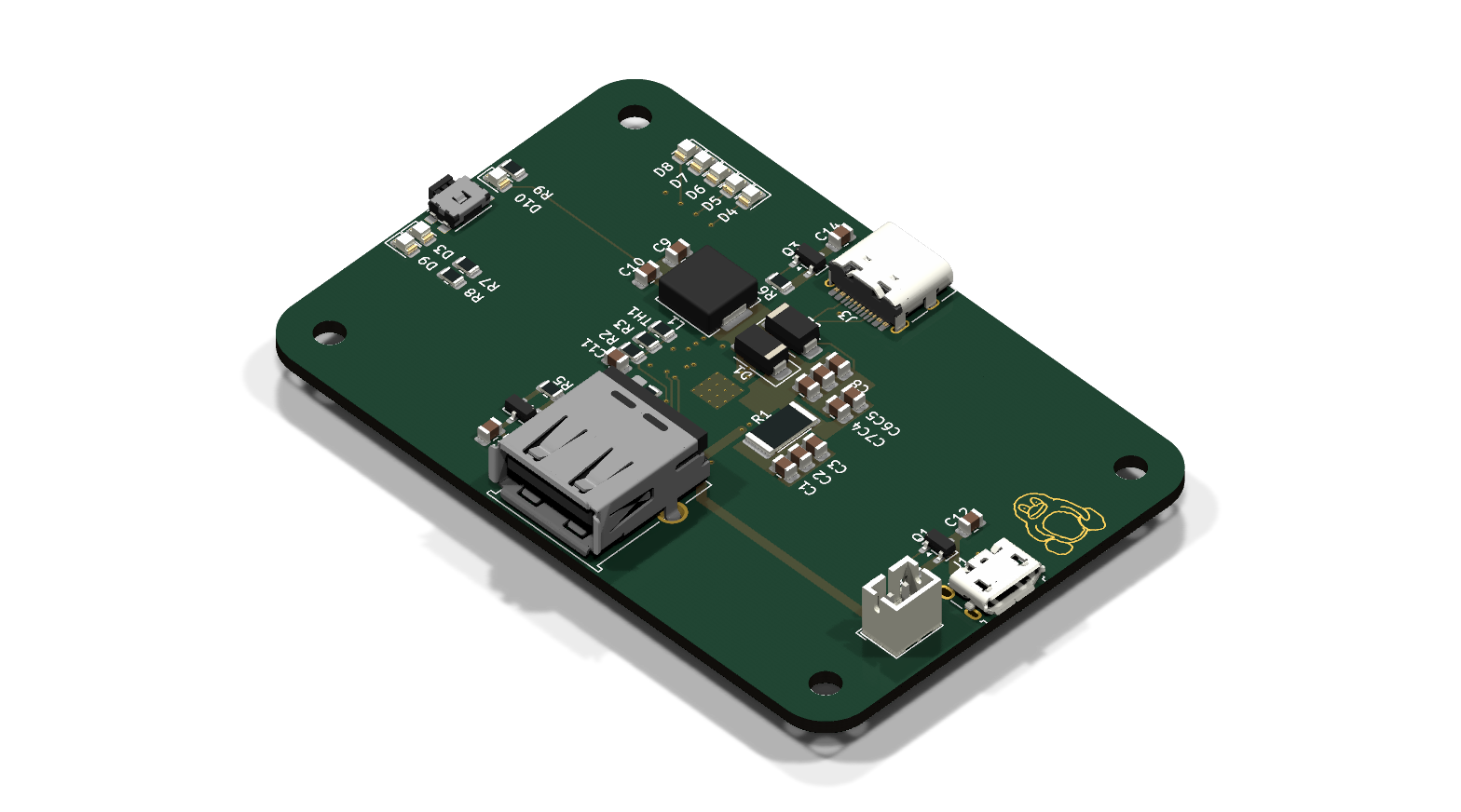
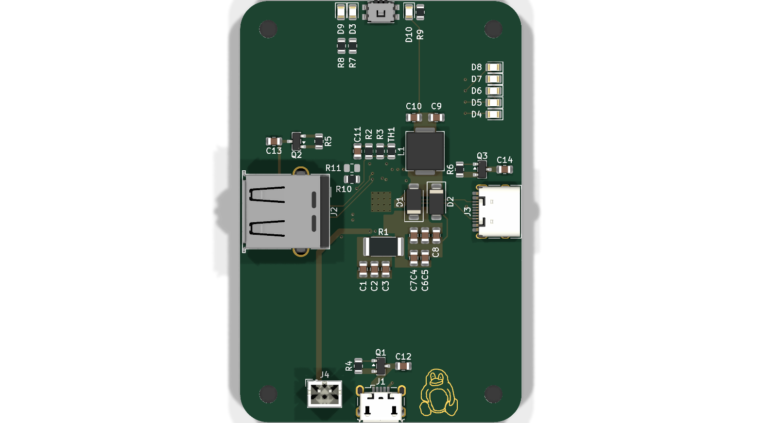
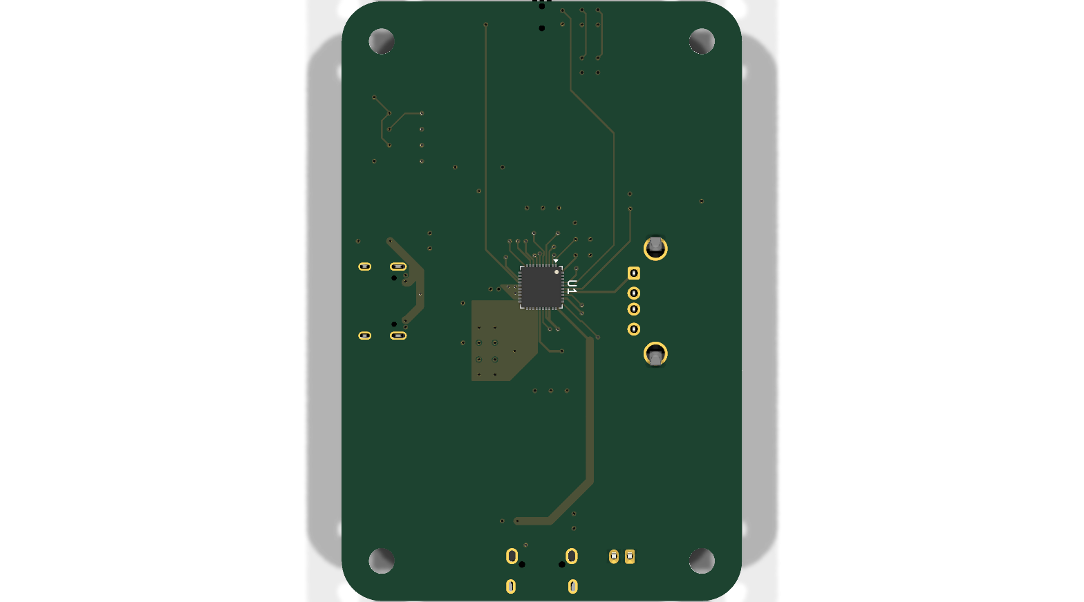
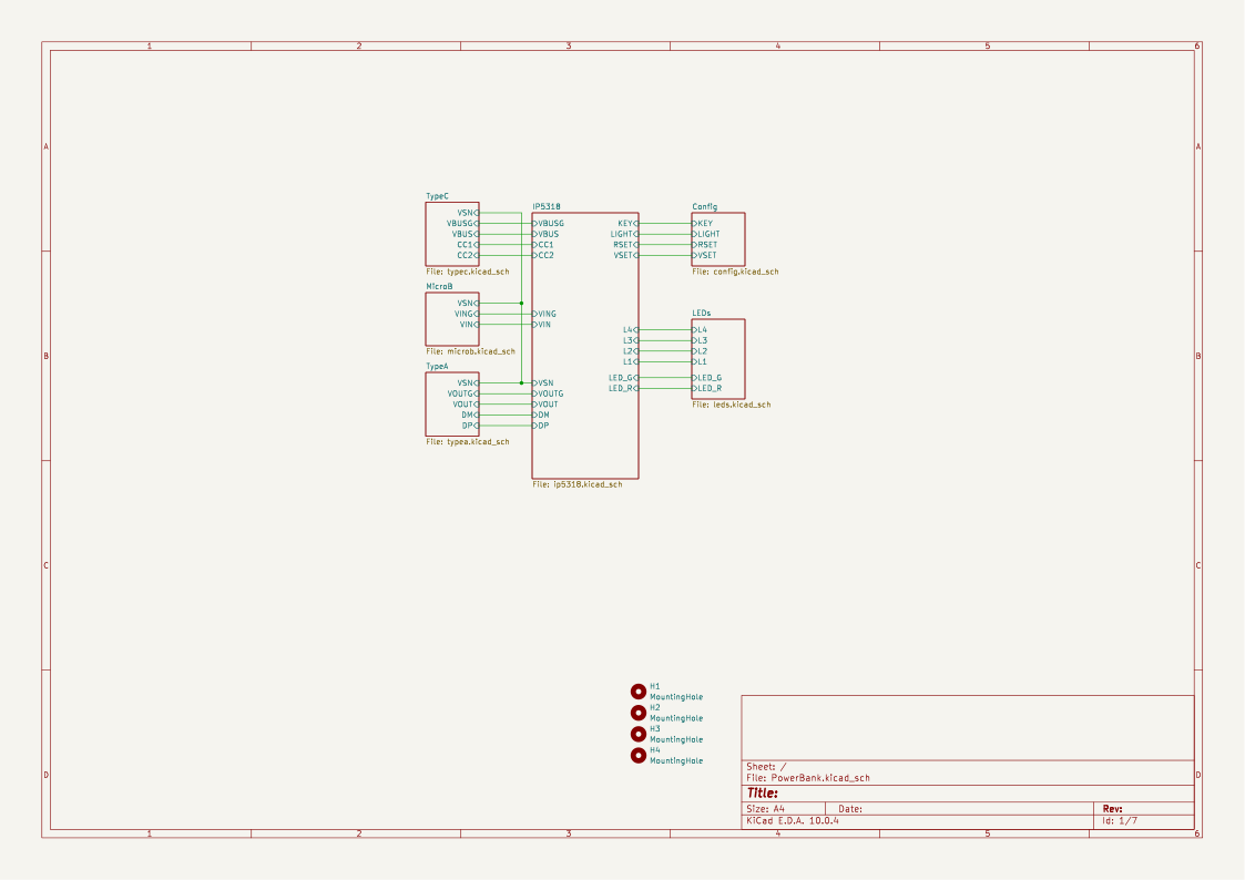
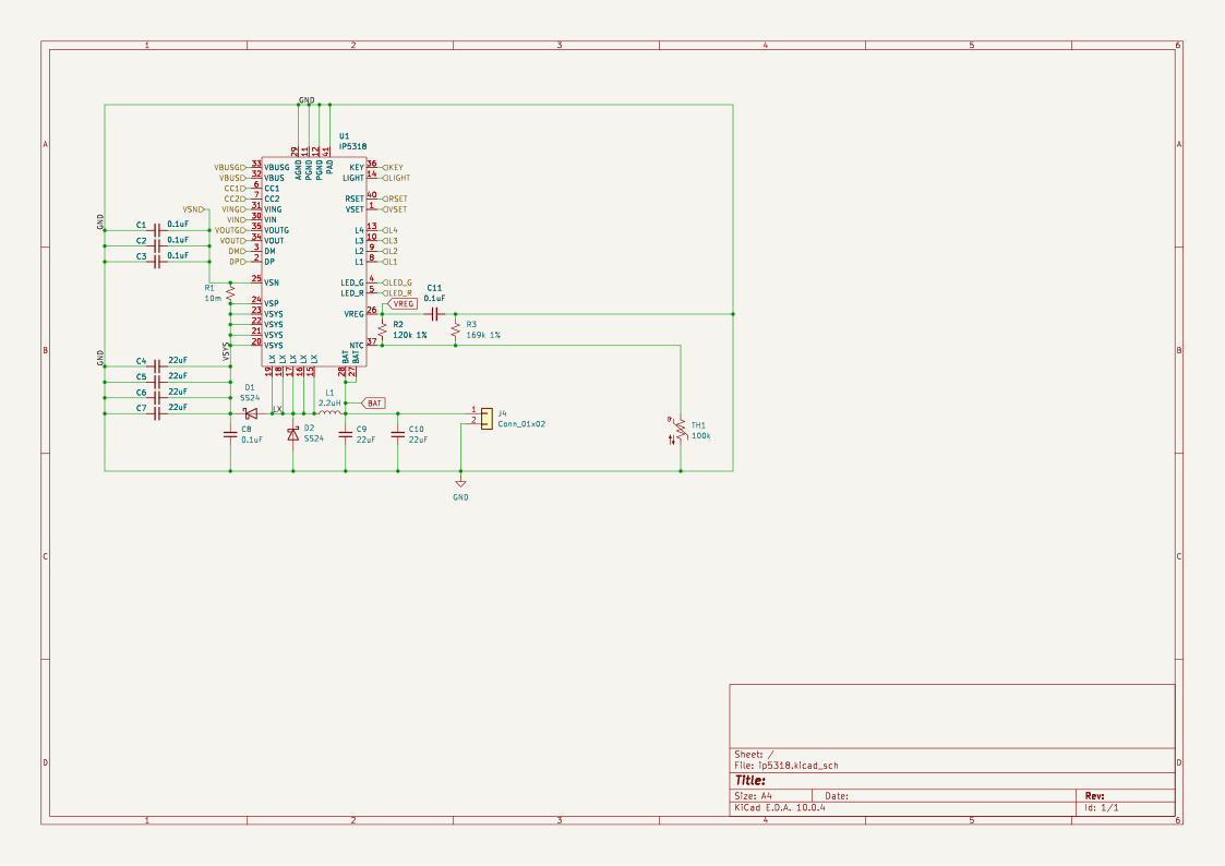
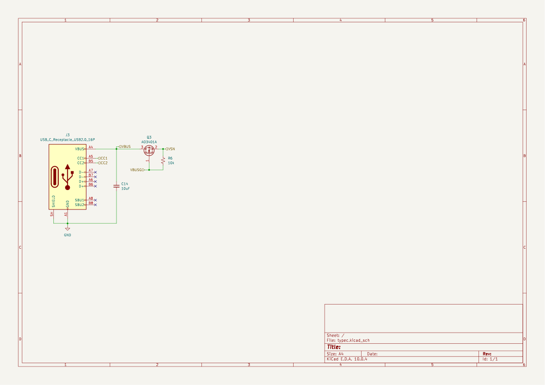
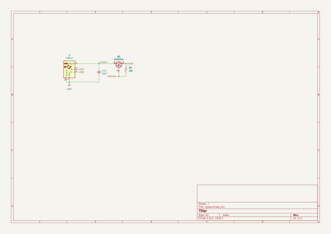
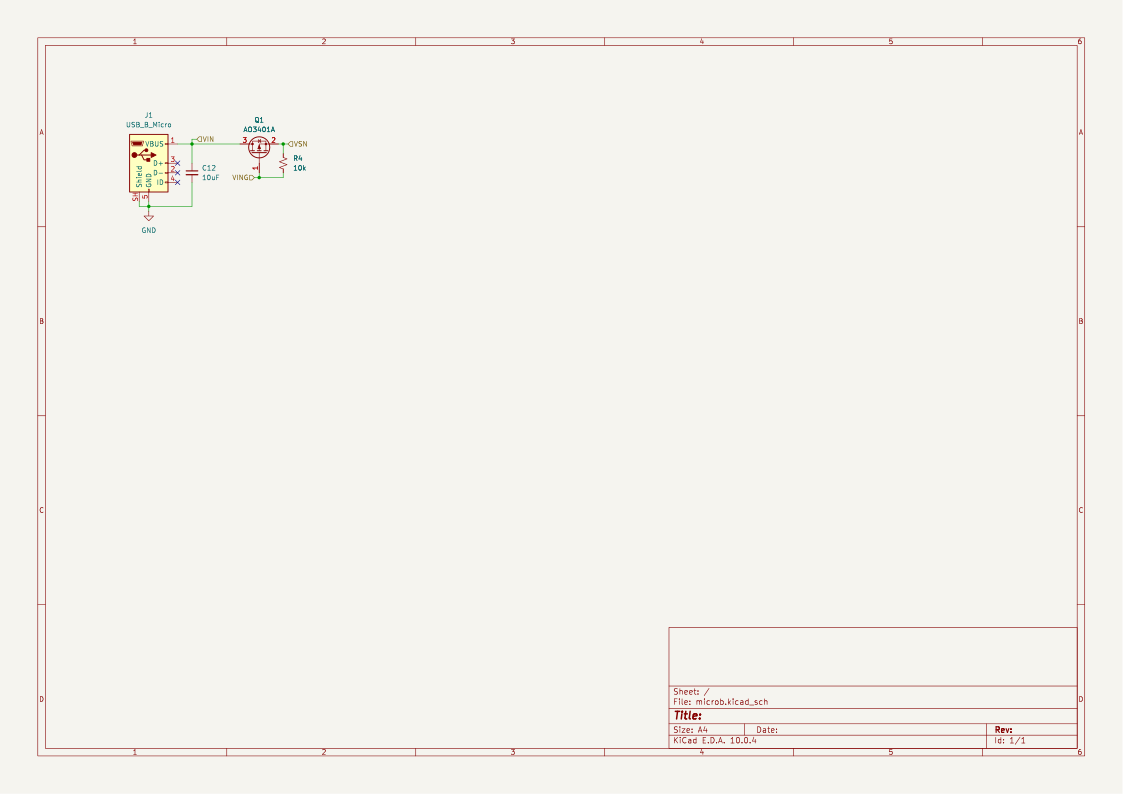
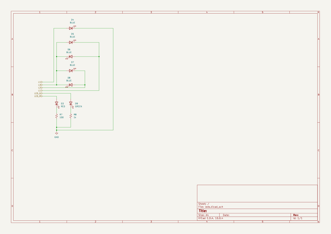
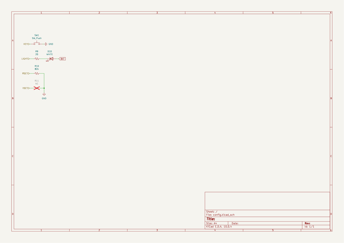
| Sheet | Description |
|---|---|
PowerBank.kicad_sch | Top-level sheet (mounting holes) |
ip5318.kicad_sch | IP5318 power bank IC and battery connections |
typec.kicad_sch | USB Type-C connector |
typea.kicad_sch | USB Type-A connector |
microb.kicad_sch | Micro-USB connector |
leds.kicad_sch | LED indicators |
config.kicad_sch | Configuration and additional LEDs |
The full BOM in BOM.csv.
| Item | Qty | Est. Cost |
|---|---|---|
| IP5318 SoC | 1 | $1.84 |
| 22uF capacitors | 6 | $1.51 |
| 10uF capacitors | 3 | $0.42 |
| 0.1uF capacitors | 5 | $0.11 |
| 2.2uH power inductor | 1 | $0.08 |
| USB Type-A connector (Molex) | 1 | $0.93 |
| USB Type-C 16-pin connector | 1 | $0.17 |
| USB Micro-B connector | 1 | $0.05 |
| JST-PH battery connector | 1 | $0.04 |
| AO3401A P-MOSFET | 3 | $0.11 |
| SS24 Schottky diodes | 2 | $0.03 |
| LEDs (0805, green/blue/red/white) | 8 | $0.10 |
| Resistors (0805) | 10 | $0.02 |
| 10m sense resistor | 1 | $0.04 |
| 100k NTC thermistor | 1 | $0.01 |
| Tactile switch | 1 | $0.23 |
| 18650 Li-ion cell (3.7V) | 1 | $2.50 |
| PCB (qty 5, JLCPCB ~84x110mm) | 5 | $6.00 |
| Total per finished board | $9.21 |
Component prices are from LCSC (Aug 2026 cart export); cell price is an AliExpress estimate. Shipping not included.
PowerBank/
├── kicad/
│   ├── PowerBank.kicad_sch
│   ├── PowerBank.kicad_pcb
│   ├── PowerBank.kicad_pro
│   ├── ip5318.kicad_sch
│   ├── typec.kicad_sch
│   ├── typea.kicad_sch
│   ├── microb.kicad_sch
│   ├── leds.kicad_sch
│   ├── config.kicad_sch
│   ├── Parts.pretty/
│   ├── fp-lib-table
│   └── production/
│       ├── PowerBank.zip (gerbers)
│       ├── bom.csv
│       ├── positions.csv
│       └── netlist.ipc
├── parts/
│   └── Parts.kicad_sym
├── cad/
│   └── PowerBank.step
├── images/
│ ├── pcb-3d-isometric.png| Qty | Value | Footprint | References |
|---|---|---|---|
| 6 | 22uF | Capacitor_SMD:C_0805_2012Metric | C4, C5, C6, C7, C9, C10 |
| 5 | 0.1uF | Capacitor_SMD:C_0805_2012Metric | C1, C2, C3, C8, C11 |
| 5 | BLUE | LED_SMD:LED_0805_2012Metric | D4, D5, D6, D7, D8 |
| 4 | MountingHole | MountingHole:MountingHole_3.2mm_M3 | H1, H2, H3, H4 |
| 3 | 10k | Resistor_SMD:R_0805_2012Metric | R4, R5, R6 |
| 3 | 10uF | Capacitor_SMD:C_0805_2012Metric | C12, C13, C14 |
| 3 | AO3401A | Package_TO_SOT_SMD:SOT-23 | Q1, Q2, Q3 |
| 2 | SS24 | Diode_SMD:D_SMA | D1, D2 |
| 1 | 100 | Resistor_SMD:R_0805_2012Metric | R7 |
| 1 | 100k | Resistor_SMD:R_0805_2012Metric | TH1 |
| 1 | 10m | Resistor_SMD:R_2512_6332Metric | R1 |
| 1 | 120k 1% | Resistor_SMD:R_0805_2012Metric | R2 |
| 1 | 169k 1% | Resistor_SMD:R_0805_2012Metric | R3 |
| 1 | 1k | Resistor_SMD:R_0805_2012Metric | R8 |
| 1 | 2.2uH | Inductor_SMD:L_APV_APH0630 | L1 |
| 1 | 20 | Resistor_SMD:R_0805_2012Metric | R9 |
| 1 | 82k | Resistor_SMD:R_0805_2012Metric | R10 |
| 1 | Conn_01x02 | Connector_JST:JST_PH_B2B-PH-K_1x02_P2.00mm_Vertical | J4 |
| 1 | GREEN | LED_SMD:LED_0805_2012Metric | D9 |
| 1 | IP5318 | Package_DFN_QFN:QFN-40-1EP_5x5mm_P0.4mm_EP3.6x3.6mm_ThermalVias | U1 |
| 1 | NC | Resistor_SMD:R_0805_2012Metric | R11 |
| 1 | RED | LED_SMD:LED_0805_2012Metric | D3 |
| 1 | SW_Push | Button_Switch_SMD:Panasonic_EVQPUM_EVQPUD | SW1 |
| 1 | USB_A | Connector_USB:USB_A_Molex_67643_Horizontal | J2 |
| 1 | USB_B_Micro | Connector_USB:USB_Micro-B_Wuerth_629105150521 | J1 |
| 1 | USB_C_Receptacle_USB2.0_16P | Connector_USB:USB_C_Receptacle_HRO_TYPE-C-31-M-12 | J3 |
| 1 | WHITE | LED_SMD:LED_0805_2012Metric | D10 |

MeesCode/gameboy-pcb
custom gameboy-esque pcb running an stm32 and my own tiny game engine


jayanta525/dual-h-bridge
Dual H-Bridge Controller with IRF3205 and IR2104 MOSFET Driver, and with ATMega328P-AU PWM Controller

Alksndr55/mesh-repeater
Mesh Repeater v1 — одноплатный LoRa-репитер для MeshCore и Meshtastic, 90×100 мм. Упор на максимальное энергосбережение и работу в суровых сибирских зимах. Солнечный зарядник, Na-ion 1S / LTO 2S.

TilenTinta/Greenhouse_LoRa_Node
An open-source monitoring system designed for use in greenhouses, orchards or other agricultural environments

Matyas604/Security-Alarm-Panel
Home Assistant Smart Home Alarm Control Panel with fingerprint reader, NFC/RFID card reader, motion radar, and touchscreen TFT display. It can control your smart home, not just your home security system.

creapunk/CLN-ClosedLoopNemaDriver
Compact closed-loop stepper motor driver designed for NEMA motors
It measures 50 × 75 mm and has 4 copper layers, 1.6 mm thick.
50 parts, built around the IP5318, AO3401A, SS24 and APH0630T2R2M. The full list of its parts is on this page, with links to each part's symbol and footprint where PCBKit's library has them.
From the sneakylizard123-4/PowerBank repository on GitHub, at the commit this page was made from: the board is kicad/_restore_backup_2026-08-18T16-52-31-033/PowerBank.kicad_pcb and its schematic kicad/PowerBank.kicad_sch. PCBKit opens the board in the browser, with nothing to install.
Its repository states no licence, so its author keeps all rights: ask sneakylizard123-4 before reusing the design.