
2 layers95.3 × 161.9 mm
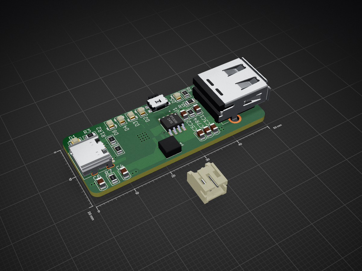
 sneakylizard123-4/IP5306_Module
A small USB power bank module that uses a 1S lithium battery and outputs a regulated 5V supply.
IP5306 Module is an open-source printed circuit board by sneakylizard123-4, from the sneakylizard123-4/IP5306_Module repository on GitHub. It is a 2-layer board of 50 × 20 mm with 27 parts on 24 nets, routed with 83 tracks and 31 vias.
It is built around the IP5306. Its parts include 7 capacitors, 7 resistors, 6 diodes, 3 connectors and 1 IC.
A small USB power bank module that uses a 1S lithium battery and outputs a regulated 5V supply.
This board is a small power bank module built around the Injoinic IP5306 SoC. It takes USB-C input to charge a lithium battery and outputs a regulated 5V rail from a USB-A port in output mode. It is a standalone module with no MCU, only a power button and 4-LED charge/fuel gauge handle all user input. I built it to have a fully integrated power path solution that avoids the complexity of discrete charger and boost circuits.
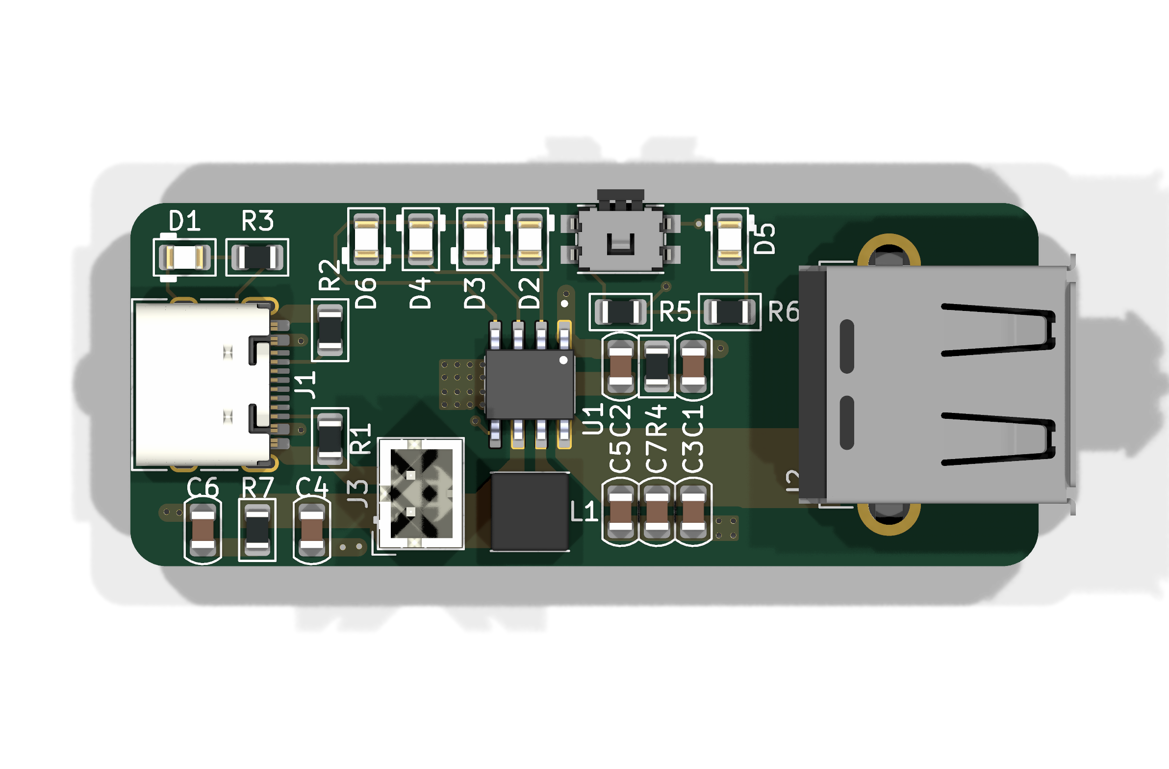
The IP5306 has an entire power path inside of it. On the input side, 5v from USB-C charges a connected 1S lithium battery through the IP5306's built-in 2.1A charger. On the output side, the chip boosts the battery voltage to a regulated 5V output rail when in power-bank mode. The boost inductor and output capacitors form the boost converter, while the battery, LED, and decoupling capacitors support the charge path, gauge, and IC supply. Pressing the KEY button powers the module on/off and goes through the fuel gauge.
| Block | Part | Role |
|---|---|---|
| Power | IP5306 | Power Bank SoC with battery charger, boost regulator, 5V rail, charge gauge |
| Input | HRO TYPE-C-31-M-12 | USB-C receptacle for charging input |
| Output | Connfly DS1095 | USB-A receptacle for 5V power-bank output |
| Battery | B2B-PH-K | JST PH 2-pin connector to 1S Li-ion/LiPo battery |
| Inductor | Coilcraft XFL4020-102MEC | 1uH boost converter inductor |
| Capacitors | 10uF x4, 22uF x3 Boost output + IC decoupling | |
| Resistors | 5.1k x2, 10k x3, 2 ohm x2 | USB-C CC pulldowns, biasing, LED current limit |
| LEDs | 0805 x6 | Charge and boost status indicators |
| Button | Panasonic EVQPUM | Power on/off + fuel gauge on KEY pin |
The power path flows from the USB-C input through the IP5306 charger into the battery, and from the battery through the IP5306 boost converter out to the USB-A port. The KEY button and LED gauge hang off the chip's control pins.
| Direction | Path |
|---|---|
| Charge | USB-C (5V) -> IP5306 charger -> 1S battery |
| Discharge | 1S battery -> IP5306 boost -> 5V USB-A out |
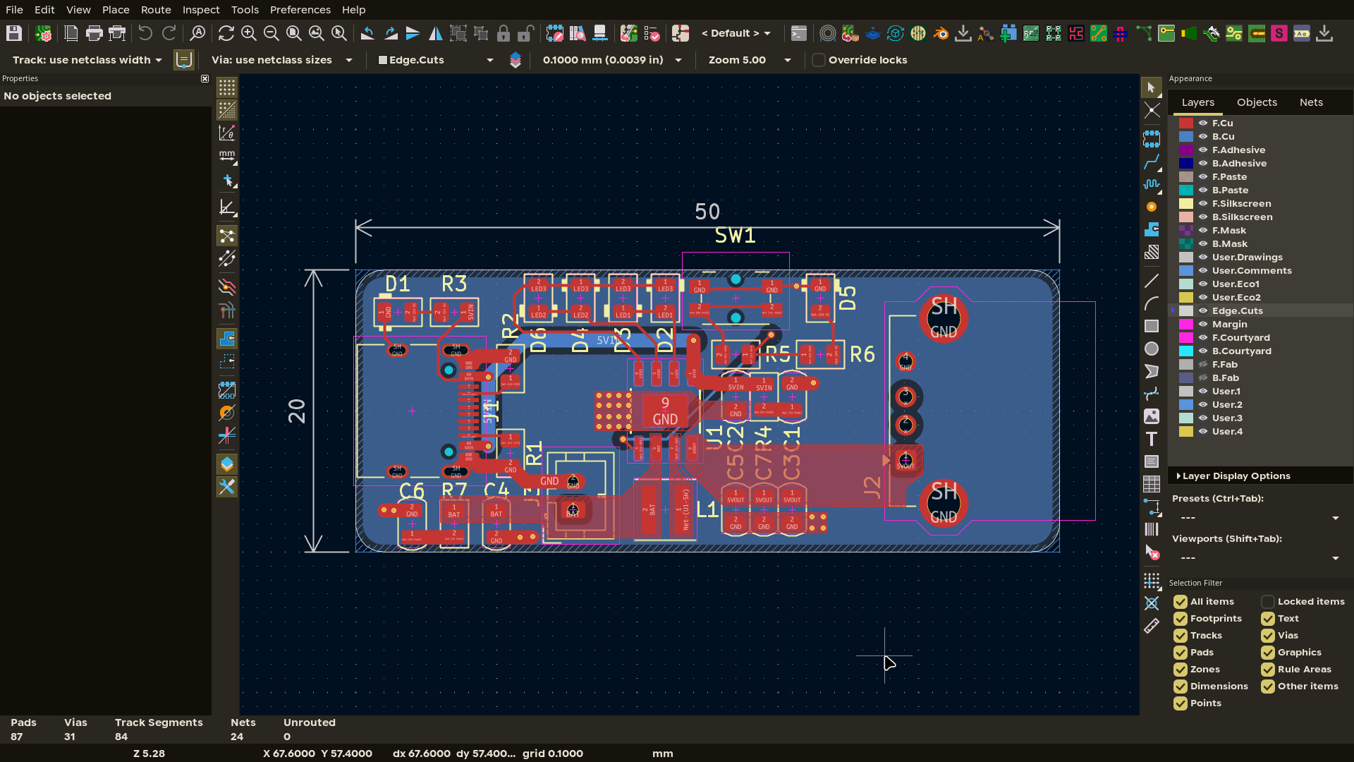
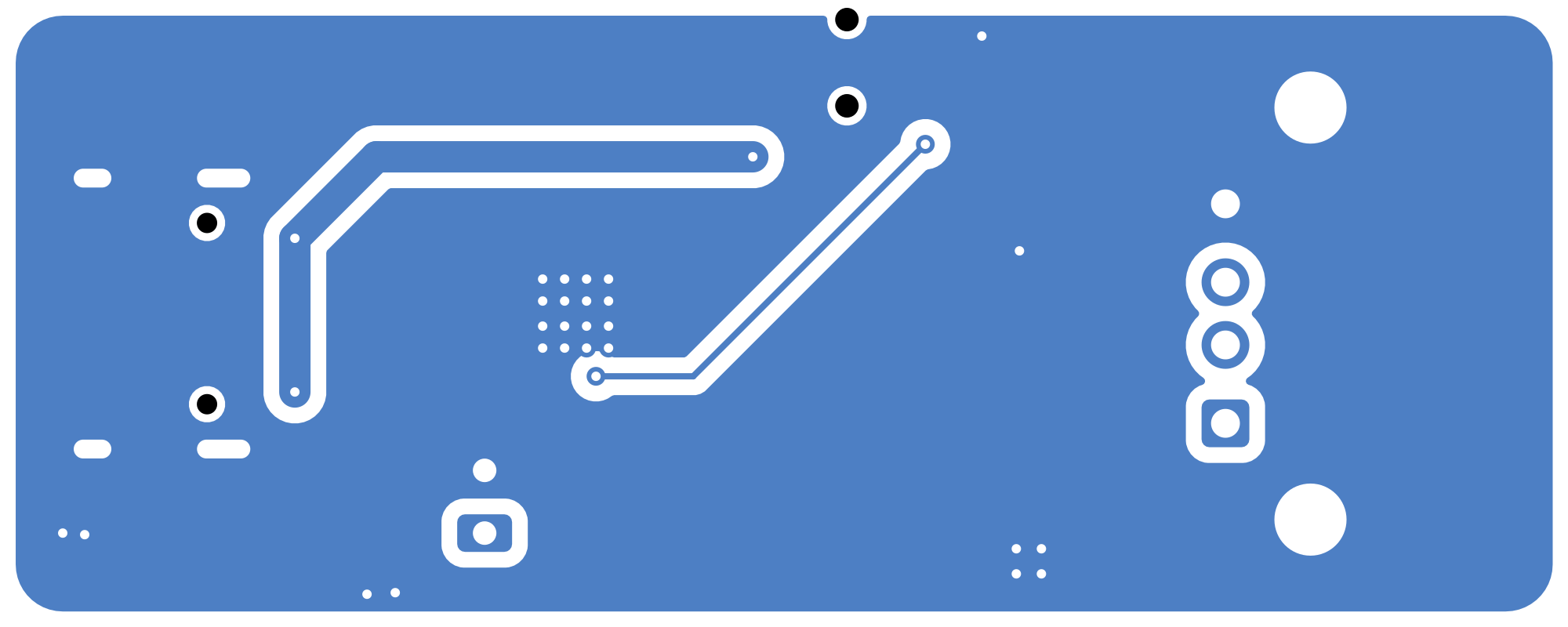
 Top layer with the tracks, pads and ground pour.
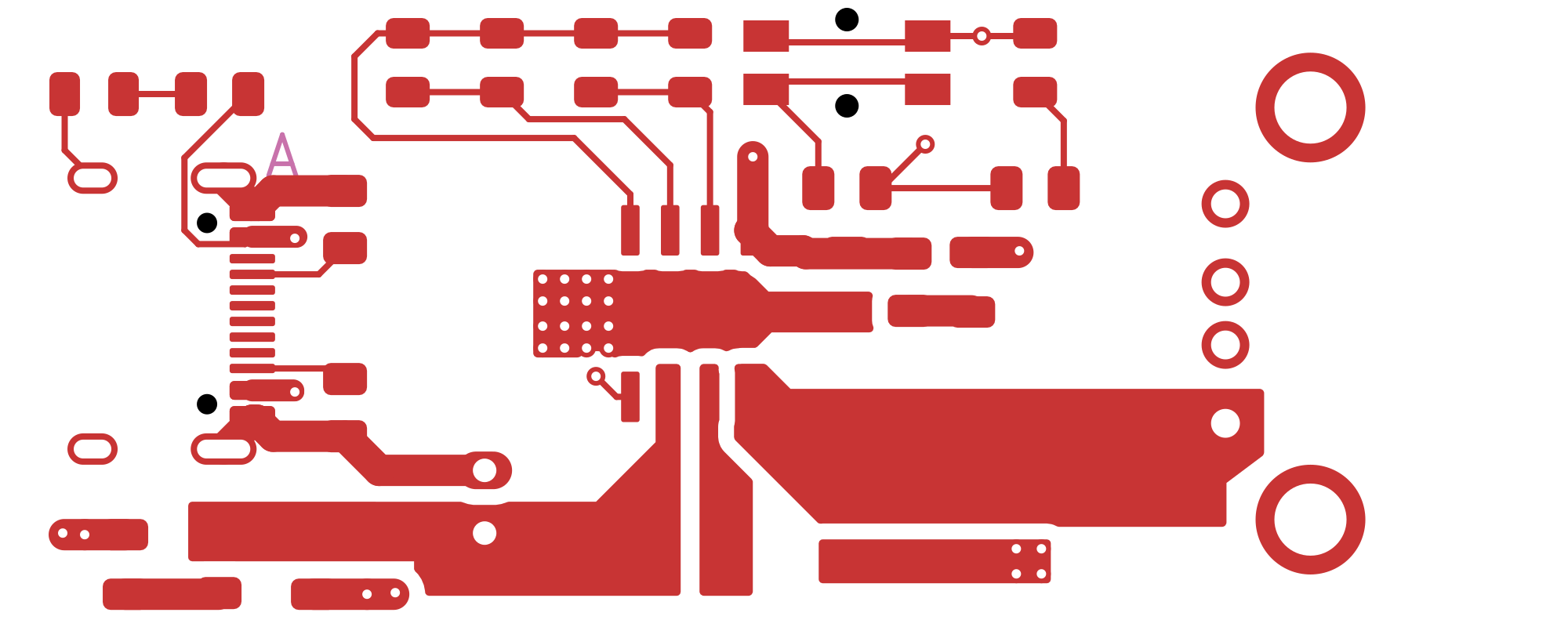
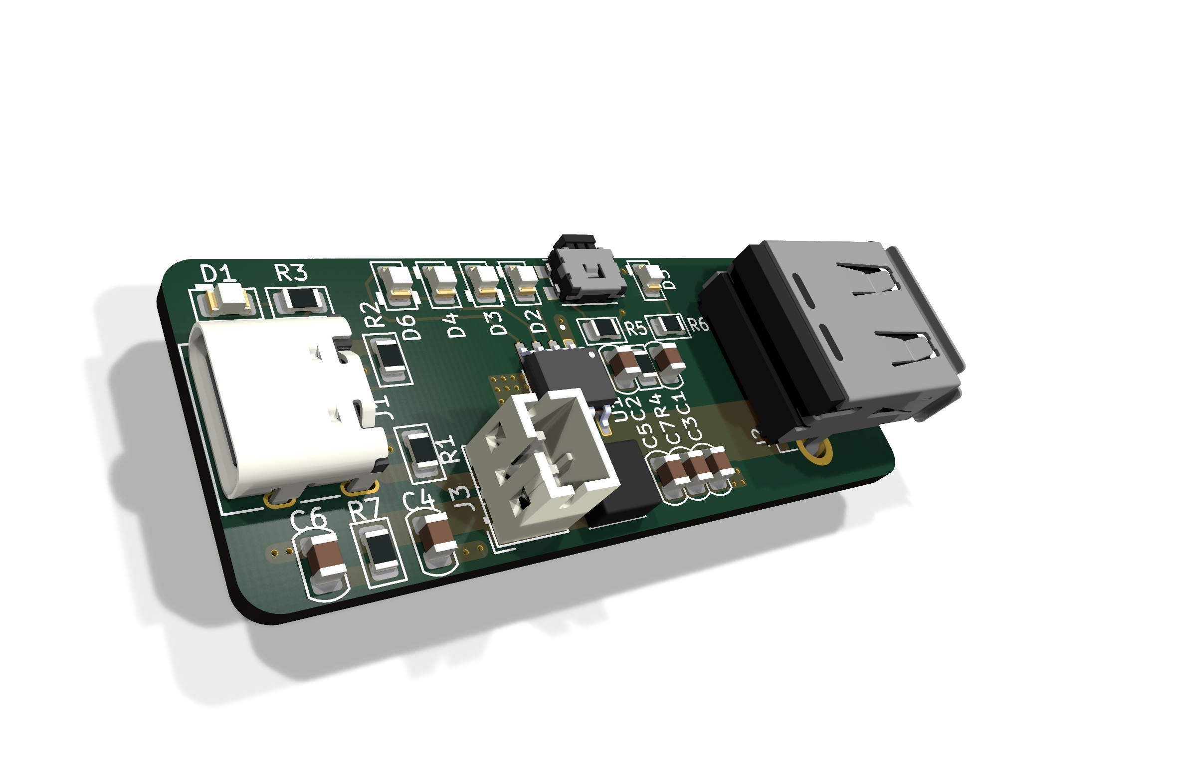
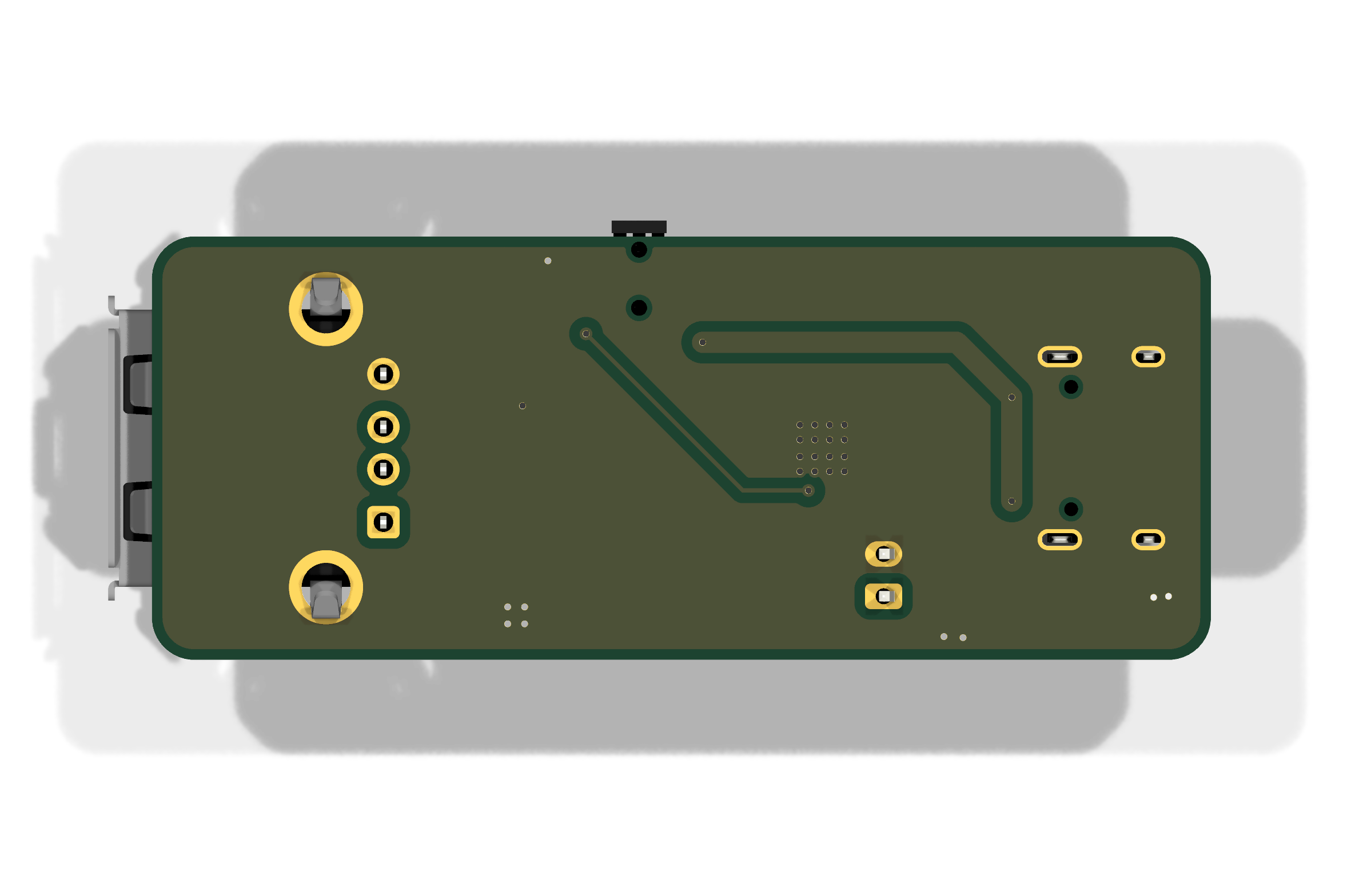
 Bottom layer with the stitched ground return path.
| Pin | Function |
|---|---|
| BAT+ / BAT- | JST PH battery connections (1S Li-ion/LiPo) |
| KEY | Power button input |
| GND | Common ground |
├── kicad/            # PCB source files
│   └── production/   # Gerbers + drill files
├── cad/              # .step export + native CAD source
├── firmware/         # Firmware source code
├── images/           # Renders, PCB screenshots, build photos
├── BOM.csv           # Bill of materials w/ links + total cost line
└── JOURNAL.md # Work journal| Item | Cost |
|---|---|
| PCB | $3.20 |
| Shipping | $1.50 |
| PCB subtotal | $4.70 |
| Components | $12.99 |
| Total | $17.69 |
Full BOM available in BOM.csv
| Qty | Value | Footprint | References |
|---|---|---|---|
| 6 | LED | LED_SMD_AKL:LED_0805_2012Metric | D1, D2, D3, D4, D5, D6 |
| 4 | 10uF | Capacitor_SMD_AKL:C_0805_2012Metric | C1, C2, C4, C6 |
| 3 | 10k | Resistor_SMD_AKL:R_0805_2012Metric | R3, R5, R6 |
| 3 | 22uF | Capacitor_SMD_AKL:C_0805_2012Metric | C3, C5, C7 |
| 2 | 2 | Resistor_SMD_AKL:R_0805_2012Metric | R4, R7 |
| 2 | 5.1k | Resistor_SMD_AKL:R_0805_2012Metric | R1, R2 |
| 1 | 1uH XFL4020-102MEC | Inductor_SMD:L_Coilcraft_XxL4020 | L1 |
| 1 | Conn_01x02 | Connector_JST_SM4:JST_PH_S2B-PH-SM4-TB_1x02-1MP_P2.00mm_Horizontal | J3 |
| 1 | IP5306 | IP5306:SOP127P600X165-9N | U1 |
| 1 | LOGO | customimages:linuxpenguin | G*** |
| 1 | SW_Push | Button_Switch_SMD:Panasonic_EVQPUM_EVQPUD | SW1 |
| 1 | USB_A | Connector_USB:USB_A_Connfly_DS1095 | J2 |
| 1 | USB_C_Receptacle_USB2.0_16P | Connector_USB:USB_C_Receptacle_HRO_TYPE-C-31-M-12 | J1 |

sh123/esp32_loraprs
LoRa ESP32 KISS Bluetooth modem (for APRSDroid or aprs.fi iOS) + APRS-IS RX/TX iGate over WiFi + Digipeater + DV (with Codec2 Walkie-Talkie)

BitDogLab/BitDogLab
Open-source educational hardware for embedded systems, programming, electronics, and physical computing.


LakoMoor/open-pocket-gbc
Game Boy / Game Boy Color on the Sipeed Tang Nano 20K: HDMI, Pocket-style menu, ST7735 LCD, USB remote. Open-source FPGA toolchain only.


Reiko0908/NeuralNetwork_Based_AutonomousCar
This project focuses on developing an autonomous car system powered by neural networks (NN). It utilizes deep learning techniques to enable key functionalities such as perception, path planning, and control.
It measures 50 × 20 mm and has 2 copper layers, 1.6 mm thick.
27 parts, built around the IP5306. The full list of its parts is on this page, with links to each part's symbol and footprint where PCBKit's library has them.
From the sneakylizard123-4/IP5306_Module repository on GitHub, at the commit this page was made from: the board is kicad/_restore_backup_2026-09-13T10-19-08-571/IP5306_Module.kicad_pcb and its schematic kicad/IP5306_Module.kicad_sch. PCBKit opens the board in the browser, with nothing to install.
Its repository states no licence, so its author keeps all rights: ask sneakylizard123-4 before reusing the design.