2 layers142.5 × 101 mm
Hillside46
mmccoyd/hillside
Family of split ergonomic keyboards with three rows of six or five keys and a generous thumb arc
92 parts448MIT

 sndsgd/sk6812-mini-e-test
PCB for verifying SK6812-MINI-E performance and power consumption
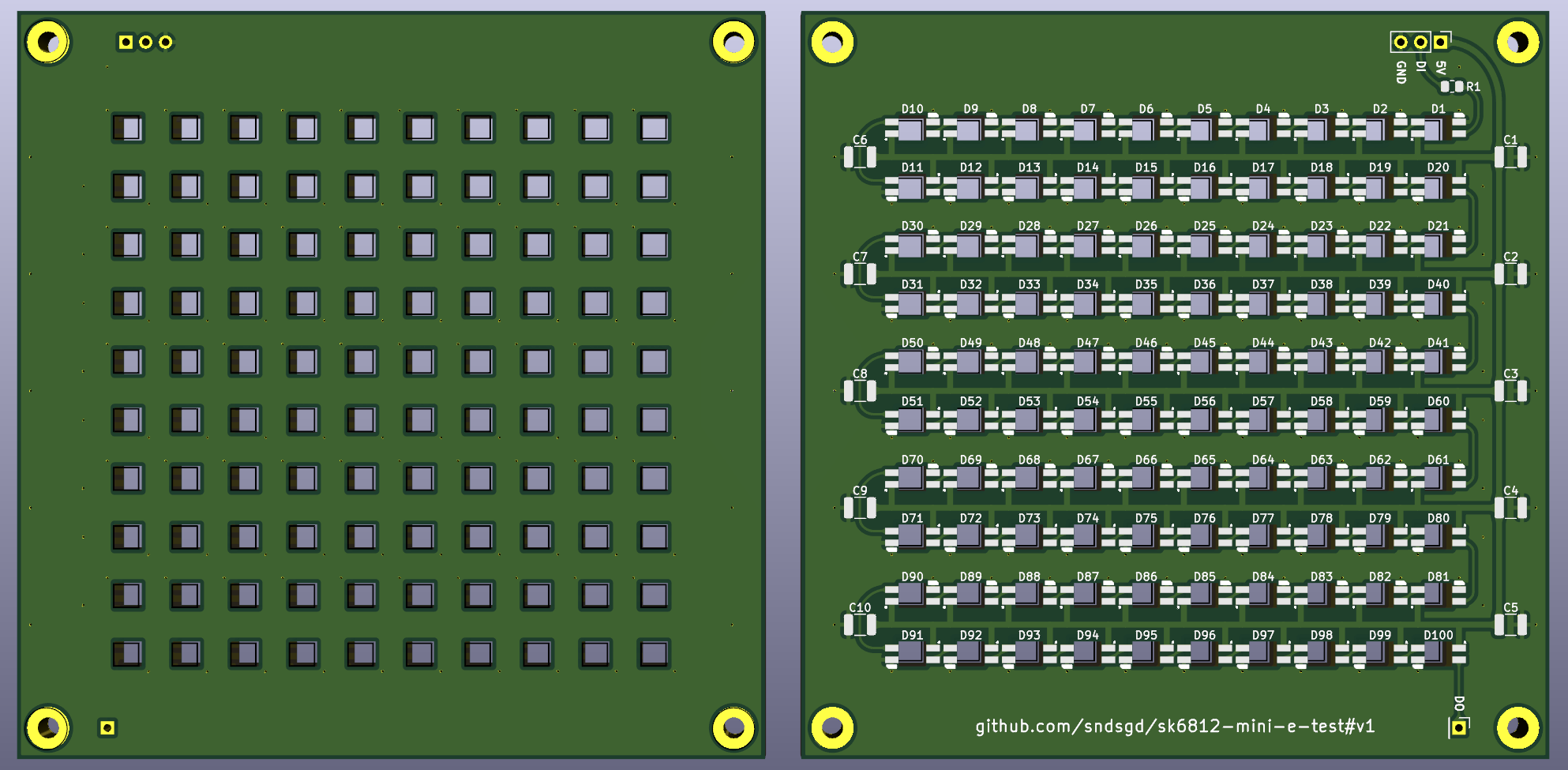
Sk6812-mini e test is an open-source printed circuit board by sndsgd, from the sndsgd/sk6812-mini-e-test repository on GitHub, published under the CERN-OHL-P-2.0 licence. It is a 2-layer board of 96 × 96 mm with 117 parts on 104 nets, routed with 628 tracks and 119 vias.
It is built around the SK6812MINI-EA and ERJ-T06J471V. Its parts include 100 diodes, 10 capacitors, 2 connectors and 1 resistor.


sk6812-mini-e-testI've successfully used SK6812-MINI-E LEDs in several projects recently, and I'm considering using lots of them in the near future. I'll be using this little board to verify performance and power requirements before scaling to thousands of LEDs.
| Qty | Value | Footprint | References |
|---|---|---|---|
| 100 | SK6812-MINI-E | project:SK6812-MINI-E-BACK | D1, D2, D10, D11, D12, D13, D14, D15, D16, D17, D18, D19, D20, D21, D22, D100 +84 |
| 10 | 100µF | Capacitor_SMD:C_1210_3225Metric | C1, C2, C3, C4, C5, C6, C7, C8, C9, C10 |
| 4 | INT | MountingHole:MountingHole_2.7mm_Pad_TopBottom | H1, H2, H3, H4 |
| 1 | 470 ohm 5% 1/4W | Resistor_SMD:R_0805_2012Metric | R1 |
| 1 | Conn_01x01_Pin | Connector_PinHeader_2.54mm:PinHeader_1x01_P2.54mm_Vertical | J2 |
| 1 | Conn_01x03_Socket | Connector_PinHeader_2.54mm:PinHeader_1x03_P2.54mm_Vertical | J1 |
mmccoyd/hillside
Family of split ergonomic keyboards with three rows of six or five keys and a generous thumb arc


Self-Made-Keyboards-in-Japan/Casasagi
The mechanical keyboard made by SMKiJ community.

It measures 96 × 96 mm and has 2 copper layers, 1.6 mm thick.
117 parts, built around the SK6812MINI-EA and ERJ-T06J471V. The full list of its parts is on this page, with links to each part's symbol and footprint where PCBKit's library has them.
From the sndsgd/sk6812-mini-e-test repository on GitHub, at the commit this page was made from: the board is sk6812-mini-e-test.kicad_pcb and its schematic sk6812-mini-e-test.kicad_sch. PCBKit opens the board in the browser, with nothing to install.
Its repository publishes it under the CERN-OHL-P-2.0 licence: you may reuse it on that licence's terms (keep the author's notice, and for a copyleft licence share your changes alike).