2 layers364 × 203 mm

 smaldragon/SillyTestRom
"SillyTestRom" is a simple discrete logic mapper for the famicom/clone that I made for my own personal messing around with homebrew, there are currently no plans to use this in anything.
SillyTestRom is an open-source printed circuit board by smaldragon, from the smaldragon/SillyTestRom repository on GitHub. It is a 2-layer board of 93 × 59.4 mm with 120 parts on 170 nets, routed with 736 tracks and 83 vias.
It is built around the 74LS153DC and 74LS377PC. Its parts include 6 ICs, 5 capacitors, 3 diodes, 1 resistor and 1 connector.


"SillyTestRom" is a simple discrete logic mapper for the famicom/clone that I made for my own personal messing around with homebrew, there are currently no plans to use this in anything.
I mainly see this as an extended AxROM, compared to similar options, the main upsides of this board are low-part count and compatibility with famiclones that don't support 4-screen mirroring.
The board can also be bodged into other configurations. Currently 2 configurations of this board are being considered (by me), A and B.
NOTE Everything here is a WIP and subject to change!
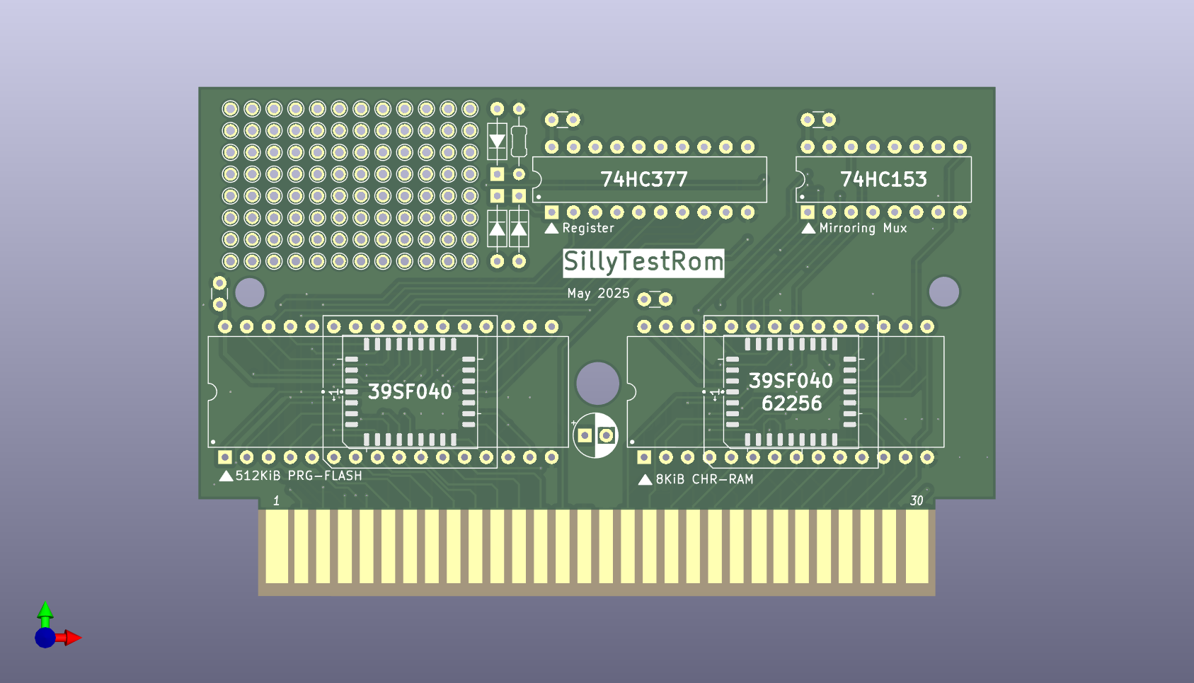
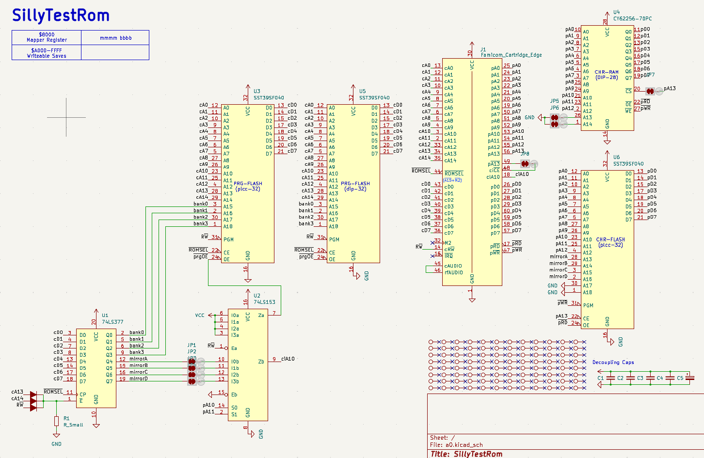
Mapper ICs:
There are no Bus Conflicts.
Its possible I may switch the PRG Bank control to use A0-3 instead, as code is always aware of which bank its currently running from, this could save code from always having to OR the graphics and bank bits together when only changing graphics values.
Data
MMMM BBBB
|    |
|    +--- PRG Bank (32K@$8000)
+-------- Nametable Mirroring

Potential Address+Data Alternative:

Address | Data
   BBBB | xxxx.MMMM
      |        +-------- Nametable Mirroring
      +----------------- PRG Bank (32K@$8000)
Each Mirroring bit controls the nametable (A or B) visible at each of the 4 logical slots, allowing for any type of (non-extended) mirroring, ie:
* $Ax -> Vertical
   AB
   AB
* $Cx -> Horizontal
   AA
   BB
* $0x -> Single Screen A
   AA
   AA
* $Fx -> Single Screen B
   BB
   BB
* $6x -> Diagonal
   AB
   BA
(etc..)The B version loses the support for horizontal and vertical mirroring, but allows for 4 CHR-RAM banks, this is motivated by the similar cost of 8KiB and 32KiB sram chips.
CCMM BBBB
| |  |
| |  +--- PRG Bank (32K@$8000)
| +------ Nametable Mirroring
+-------- CHR Bank (8K@ppu$0000)

Potential Address+Data Alternative:

Address | Data
   BBBB | xxCC.xxMM
      |     |    +------ Nametable Mirroring
      |     +----------- CHR Bank (8K@ppu$0000)
      +----------------- PRG Bank (32K@$8000)
In this case the mirroring bits are as follows:
(bits)
* 00: AA
      AA

* 01: BA
      AB

* 10: AB
      BA

* 11: BB
BBThis area is available for writing data to the 39sf flash chip. Check the datasheet for info on how this is done.
| Qty | Value | Footprint | References |
|---|---|---|---|
| 96 | TestPoint | Library:TestPoint_THTPad_D1.5mm_Drill1mm | TP1, TP2, TP10, TP11, TP12, TP13, TP14, TP15, TP16, TP17, TP18, TP19, TP20, TP21, TP22, TP23 +80 |
| 8 | SolderJumper_2_Bridged | Jumper:SolderJumper-2_P1.3mm_Bridged2Bar_RoundedPad1.0x1.5mm | JP1, JP2, JP3, JP4, JP5, JP6, JP7, JP8 |
| 4 | C_Small | Capacitor_THT:C_Disc_D3.0mm_W1.6mm_P2.50mm | C1, C2, C3, C4 |
| 3 | 1N4148 | PCM_Diode_THT_AKL:D_DO-35_SOD27_P7.62mm_Horizontal | D1, D2, D3 |
| 2 | SST39SF040 | PCM_Package_LCC_AKL:PLCC-32_SMD-Socket | U3, U6 |
| 1 | 74LS153 | PCM_Package_DIP_AKL:DIP-16_W7.62mm | U2 |
| 1 | 74LS377 | PCM_Package_DIP_AKL:DIP-20_W7.62mm | U1 |
| 1 | CY62256-70PC | PCM_Package_DIP_AKL:DIP-28_W15.24mm | U4 |
| 1 | C_Polarized_Small | Capacitor_THT:CP_Radial_D5.0mm_P2.50mm | C5 |
| 1 | Famicom_Cartridge_Edge | famicom:Famicom Cartridge Edge Connector (long legs) | J1 |
| 1 | R_Small | PCM_Resistor_THT_AKL:R_Axial_DIN0204_L3.6mm_D1.6mm_P7.62mm_Horizontal | R1 |
| 1 | SST39SF040 | PCM_Package_DIP_AKL:DIP-32_W15.24mm | U5 |

jes/scamp-cpu
A homebrew 16-bit CPU with a homebrew Unix-like-ish operating system.

MouseBiteLabs/NES-Cartridges
A collection of Nintendo Entertainment System (NES) cartridge circuit boards

digilogistist/The-Open-Source-USB-NES-Project
USB-NES and NES-FASTGFX product engineering repository


reinvantveer/68KatyClone
An open-hardware design for an 8-bit Motorola 68008 system

Robert-Mones/Claculator
A reverse Polish notation calculator with added features such as comparisons, branching, and custom recursive operators taken from the Clac project from the 15-122 course at Carnegie Mellon University.

adasneves127/SAFETy-Computer
A full Turing Complete computer made from TTL components
It measures 93 × 59.4 mm and has 2 copper layers, 1.2 mm thick.
120 parts, built around the 74LS153DC and 74LS377PC. The full list of its parts is on this page, with links to each part's symbol and footprint where PCBKit's library has them.
From the smaldragon/SillyTestRom repository on GitHub, at the commit this page was made from: the board is Kicad/a0/a0.kicad_pcb and its schematic Kicad/a0/a0.kicad_sch. PCBKit opens the board in the browser, with nothing to install.
Its repository states no licence, so its author keeps all rights: ask smaldragon before reusing the design.