2 layers339.1 × 143.2 mm
Adelheid
dcpedit/adelheid-plus
The Adelheid Plus is a fork of Flookay's Adelheid case and PCB.
332 parts28MIT

 slagnt/thin_pcb
5x5 pcb atmega32u4 smd
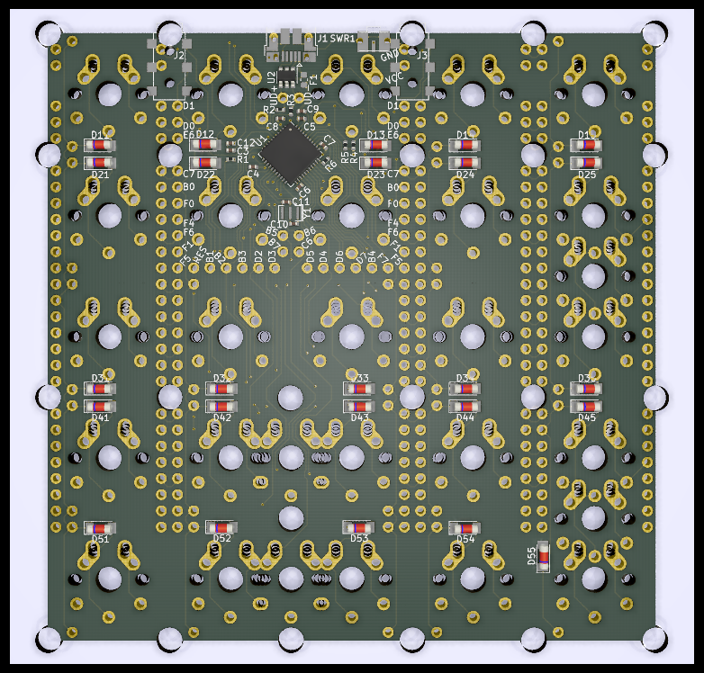
Thin pcb is an open-source printed circuit board by slagnt, from the slagnt/thin_pcb repository on GitHub. It is a 2-layer board of 95.3 × 95.3 mm with 225 parts on 70 nets, routed with 2,676 tracks and 243 vias.
It is built around the ATMEGA32U4-MU and USBLC6-2SC6. Its parts include 90 connectors, 29 switches, 25 diodes, 10 capacitors and 6 resistors. It belongs with the AVR (ATmega, ATtiny) boards of this library.


| Qty | Value | Footprint | References |
|---|---|---|---|
| 45 | Conn_01x01 | lib:PinSocket_1x01_P2.54mm_Vertical | J111, J115, J121, J124, J125, J131, J132, J133, J134, J141, J142, J143, J144, J145, J151, J152 +29 |
| 27 | SW_Push | lib:MX-Alps-Choc-1U-Mine | SW11, SW12, SW13, SW14, SW15, SW21, SW22, SW23, SW24, SW25, SW31, SW32, SW33, SW34, SW35, SW252 +11 |
| 25 | D | Diode_SMD:D_MiniMELF | D11, D12, D13, D14, D15, D21, D22, D23, D24, D25, D31, D32, D33, D34, D35, D41 +9 |
| 23 | MountingHole | MountingHole:MountingHole_4mm | H00, H01, H03, H04, H05, H10, H11, H13, H14, H15, H30, H31, H32, H33, H34, H35 +7 |
| 16 | Conn_01x07 | lib:PinSocket_1x07_P2.54mm_Vertical | J21, J22, J23, J24, J25, J26, J27, J28, J31, J32, J33, J34, J35, J36, J37, J38 |
| 8 | Conn_01x03 | lib:PinSocket_1x03_P2.54mm_Vertical | J11, J12, J13, J14, J15, J16, J17, J18 |
| 8 | Conn_01x04 | lib:PinSocket_1x07_P2.54mm_Vertical | J41, J42, J43, J44, J45, J46, J47, J48 |
| 7 | Conn_01x02 | lib:PinSocket_1x02_P2.54mm_Vertical | J01, J02, J04, J06, J07, J7, J08 |
| 6 | , , , , , | ||
| 5 | 0.1u | Capacitor_SMD:C_0402_1005Metric | C4, C5, C6, C7, C9 |
| 4 | 10k | Resistor_SMD:R_0402_1005Metric | R1, R4, R5, R6 |
| 2 | 10p | Capacitor_SMD:C_0402_1005Metric | C10, C11 |
| 2 | 22 | Resistor_SMD:R_0402_1005Metric | R2, R3 |
| 2 | AudioJack4_Ground | lib:Jack_2.5mm_PJ242 | J2, J3 |
| 2 | Conn_01x06 | lib:PinSocket_1x06_P2.54mm_Vertical | J4, J5 |
| 2 | SW_Push | lib:MX-Alps-Choc-1U-Mine-Flip | SW422, SW522 |
| 1 | 100u | Capacitor_SMD:C_0402_1005Metric | C12 |
| 1 | 10u | Capacitor_SMD:C_0402_1005Metric | C8 |
| 1 | 1u | Capacitor_SMD:C_0402_1005Metric | C3 |
| 1 | 500m | Fuse:Fuse_0603_1608Metric | F1 |
| 1 | ATmega32U4-MU | Package_DFN_QFN:QFN-44-1EP_7x7mm_P0.5mm_EP5.2x5.2mm | U1 |
| 1 | Conn_02x02 | lib:PinSocket_2x02_P2.54mm_Vertical | J6 |
| 1 | Crystal | Crystal:Resonator_SMD_muRata_CSTxExxV-3Pin_3.0x1.1mm | Y1 |
| 1 | SW_Push | lib:SW_Reset | SWR1 |
| 1 | USBLC6-2SC6 | Package_TO_SOT_SMD:SOT-23-6 | U2 |
| 1 | USB_B_Micro | Connector_USB:USB_Micro-B_Amphenol_10103594-0001LF_Horizontal | J1 |
The 194 most common of 225 parts.
It measures 95.3 × 95.3 mm and has 2 copper layers, 1.6 mm thick.
225 parts, built around the ATMEGA32U4-MU and USBLC6-2SC6. The full list of its parts is on this page, with links to each part's symbol and footprint where PCBKit's library has them.
From the slagnt/thin_pcb repository on GitHub, at the commit this page was made from: the board is thin_pcb.kicad_pcb. PCBKit opens the board in the browser, with nothing to install.
Its repository states no licence, so its author keeps all rights: ask slagnt before reusing the design.
dcpedit/adelheid-plus
The Adelheid Plus is a fork of Flookay's Adelheid case and PCB.


ghostseven/Draytronics-Elise-PCB-V2
(Current V2) An open source 65% mechanical keyboard, designed to be physically compatible with XD68


hackclub/OnBoard
💡 Join 1,000 teenagers and make your first PCB with a $100 grant!