2 layers65 × 56 mm

 sittner/sl56660
The Fairchild SL56660 is one of the small set of logic building blocks the Cray-1 supercomputer (1976) was made of: a dual NAND gate (one 5-input, one 4-input) with complementary outputs, implemented in emitter-coupled…
Sl56660 is an open-source printed circuit board by sittner, from the sittner/sl56660 repository on GitHub, published under the CERN-OHL-W-2.0 licence. It is a 2-layer board of 22 × 13 mm with 25 parts on 25 nets, routed with 106 tracks and 25 vias.
It is built around the ATTINY4-TSH, 1N5819HW and BC856BDW1. Its parts include 14 resistors, 5 diodes, 2 ICs, 2 connectors and 1 capacitor. It belongs with the AVR (ATmega, ATtiny) boards of this library.


The Fairchild SL56660 is one of the small set of logic building blocks the Cray-1 supercomputer (1976) was made of: a dual NAND gate (one 5-input, one 4-input) with complementary outputs, implemented in emitter-coupled logic (ECL) in a 16-pin ceramic flatpack.
I got one as part of the "First Super Computer" kit from Mini Museum — a lovely display piece for the bookshelf, but I missed some action. Since no datasheet, pinout or schematic for the part is in public circulation, I reverse-engineered the pinout from bench measurements and then designed a small demo board that lets the chip do again what it did in the Cray-1: switch.
Project status: the pinout is verified on real hardware, the board is
fully designed and the ATtiny firmware is written
(avr-firmware/) — but the board is not built yet, so the
firmware has only been compiled, never run on hardware.
ECL cannot be probed like TTL: it runs on a negative supply (VEE = −5.2 V) with VCC at ground, the signal swing is small (≈ −0.9 V / −1.75 V, with the Cray using negative logic: logic 1 is the more negative level — that convention is what makes this OR/NOR hardware a NAND gate), and the outputs are open emitters that need external pull-downs. Applying power to the wrong pins would kill the die, so the pinout was recovered non-destructively first:
The full write-up, including the measurement matrices, the reasoning behind
each conclusion and the verified pinout, is in
SL56660_reverse_engineering.md.
| Pin | Signal | Pin | Signal | |
|---|---|---|---|---|
| 1 | in A1 | 9 | in B2 | |
| 2 | out A (NAND) | 10 | in B3 | |
| 3 | out A (AND) | 11 | in B4 | |
| 4 | Vcc2 (current switch, GND) | 12 | Vee (−5.2 V) | |
| 5 | Vcc1 (output followers, GND) | 13 | in A5 | |
| 6 | out B (AND) | 14 | in A4 | |
| 7 | out B (NAND) | 15 | in A3 | |
| 8 | in B1 | 16 | in A2 |
Gate A is the 5-input NAND (inputs 1, 13–16), Gate B the 4-input NAND (inputs 8–11). Inputs have internal ~36 kΩ pull-downs to VEE (an open input floats to logic 1, which is neutral for a NAND); outputs are open emitters and need external pull-downs to VEE.
The two NAND gates are cross-coupled into a classic bistable flip-flop (set/reset latch) — the exact role such gates played in the Cray-1. Around it:
Power comes in through J101: a single negative rail (VEE) against GND, as in the original machine. In practice an ordinary external 5 V supply does the job — connected with its positive terminal to the board's GND and its negative terminal to VEE, it yields VEE = −5 V, close enough to the nominal −5.2 V. The D105 clamp only survives what the supply can deliver, so use a current-limited supply (or a small polyfuse in the feed, e.g. 250–500 mA hold — the board draws only ~60 mA).
The board is deliberately tiny: it is meant to go back inside the Mini Museum display case together with the chip, fed through thin enamelled copper wires from the external supply, so the display piece keeps its looks but finally blinks.
| Top | Bottom |
|---|---|
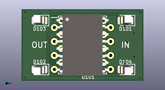 | 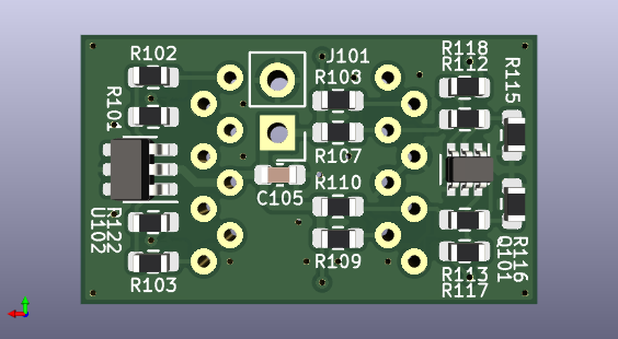 |
| File | Description |
|---|---|
SL56660_reverse_engineering.md | Full reverse-engineering write-up: method, measurement matrices, analysis, verified pinout |
ECL.svg | Basic ECL gate schematic (Gerry Ashton, CC BY-SA 3.0, via Wikimedia Commons) |
SL56660.kicad_pro / .kicad_sch / .kicad_pcb | KiCad project, schematic and board layout of the demo circuit |
SL56660.pdf | Schematic as PDF |
SL56660-top.png / SL56660-bot.png | Rendered board views |
LICENSE | CERN-OHL-W-2.0 license text |
This project is licensed under the
CERN Open Hardware Licence Version 2 — Weakly Reciprocal
(CERN-OHL-W-2.0). See LICENSE for the full text.
If you have one of these chips and want to repeat this: never apply power before you are sure of the supply pins. ECL parts are unforgiving — VEE on the wrong pin destroys the die instantly, and these dice stopped being made almost fifty years ago. Follow the unpowered-first method in the write-up.
| Qty | Value | Footprint | References |
|---|---|---|---|
| 4 | 1k2 | Resistor_SMD:R_0603_1608Metric | R101, R117, R118, R122 |
| 4 | 510R | Resistor_SMD:R_0603_1608Metric | R107, R108, R109, R110 |
| 4 | 8k2 | Resistor_SMD:R_0603_1608Metric | R102, R103, R112, R113 |
| 4 | LED | LED_SMD:LED_0805_2012Metric | D101, D102, D103, D104 |
| 2 | 10k | Resistor_SMD:R_0603_1608Metric | R115, R116 |
| 1 | 100n | Capacitor_SMD:C_0603_1608Metric | C105 |
| 1 | 1N5819HW | Diode_SMD:D_SOD-123 | D105 |
| 1 | ATtiny4-TS | Package_TO_SOT_SMD:SOT-23-6 | U102 |
| 1 | BC856BDW1 | Package_TO_SOT_SMD:SOT-363_SC-70-6 | Q101 |
| 1 | Power | Connector_PinHeader_2.54mm:PinHeader_1x02_P2.54mm_Vertical | J101 |
| 1 | Prog | Connector_PinSocket_1.27mm:PinSocket_1x05_P1.27mm_Vertical | J102 |
| 1 | SL56660 | modusoft:CFP-16_6.4x9.7mm_P1.27mm | U101 |
It measures 22 × 13 mm and has 2 copper layers, 1.6 mm thick.
25 parts, built around the ATTINY4-TSH, 1N5819HW and BC856BDW1. The full list of its parts is on this page, with links to each part's symbol and footprint where PCBKit's library has them.
From the sittner/sl56660 repository on GitHub, at the commit this page was made from: the board is SL56660.kicad_pcb and its schematic SL56660.kicad_sch. PCBKit opens the board in the browser, with nothing to install.
Its repository publishes it under the CERN-OHL-W-2.0 licence: you may reuse it on that licence's terms (keep the author's notice, and for a copyleft licence share your changes alike).


westlicht/performer-hardware
PER|FORMER Eurorack Sequencer - Hardware Design Files

sarnesjo/nearness
Minimal panning mixer for the Eurorack modular synthesizer system

rogerclarkmelbourne/STM32_Pill_Boards
Various STM32 boards in a form factor similar to the Maple Mini or Blue Pill board