

2 layers151 × 150.7 mm

 simon-frankau/dumb-vga2
Hardware to generate a simple VGA-like video display using little more than a memory chip and counters
Dumb vga is an open-source printed circuit board by simon-frankau, from the simon-frankau/dumb-vga repository on GitHub, published under the MIT licence. It is a 2-layer board of 62.2 × 83.8 mm with 26 parts on 60 nets, routed with 331 tracks and 3 vias.
It is built around the 74HC590N112 and 74HC574N. Its parts include 6 capacitors, 6 resistors, 5 ICs, 3 connectors and 1 crystal. It belongs with the lEDs and displays boards of this library.
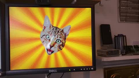
The idea of this project is to generate a basic VGA-like signal that a monitor will display by putting the signal in a flash memory, and then using counters to run through the address space. Simple, eh?
We have h-sync and v-sync signals, with their respective front and back porches. The main trick is the find a resolution that fits nicely into a flash memory, so that the flash memory is a multiple of the screen size - not the visible screen size, but the screen size with all the sync bits.
A bit of twiddling gives a 384x240 visible display that is 512x256 once all the sync etc. is factored in.
A 32MHz clock is used as a dot clock for a 768x480 image at 60 FPS (1024x512 when sync signals are factored in). The Flash cannot handle a 32MHz data rate, but we clock it every other cycle and do scan-line doubling to display a 384x240 image.
H- and V-sync signals are straightforward to produce, as they're apparently supposed to be TTL. That leaves 6 bits for 3 channels of colour, or 2 bits per channel. A pair of resistors on each channel makes the world's simplest DAC, with values chosen to give a 0.7V peak when terminated by a 75 ohm resistor when both bits are set.
gen_test.lua generates a simple RGB "checkerboard" displaying the range of available colours.
gen_rom.lua generates a ROM image given a Gimp .data file (I couldn't find a nice low-dep Lua image library). It simply takes the top two bits of each pixel value to generate the colour.
prep_img.lua converts a .data image into another .data image that uses the 6-bit colour space that the circuit can display. It uses dithering to improve the generated image. Generating a ROM image from an image that has been prepared with 'prep_img' should produce a rather better result.
The circuit breadboarded so far has three chained 74HC counters supplying the address to a 29040 flash chip. A 74HC574 latches the values for the display. (A 74HC574 triggers on the wrong edge to avoid transients, but it's what I had to hand, and seems to work fine.)
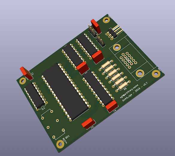
I sent the files in hw/gerbers to http://smart-prototyping.com/, and they quickly sent me back PCBs which did the job. There are PDFs of the Gerbers in hw/images.
The PCB is pretty straightforward to assemble (no surface mount!) as long as you pay attention to the orientations, as I oriented things to make routing easy, rather than assembly.
There should be enough space for a ZIF for the flash chip, although I only used an IC socket.
The PCB has been designed to support 8-pin-sized oscillators as well as 14-pin-sized oscillators. However, I installed the larger size. Take a careful look at the PCB to see how to install the smaller crystal if that's what you have. Check that power and ground reach the appropriate pins.
Note that pin 1 of the power connector is ground, and pin 3 is Vcc. This is something I wasn't paying attention to when setting up the schematic (nor did I label it on the silkscreen).
There are two headers on the board that you can jumper to set the animation speed. They look like this:
 . . .   . . .
   P3      P2
The possibilities are:
 === .   === . Slow

 === .   . === Medium

 . ===   . === Fast
Note that only "medium" displays the 4 frames in the order they are in memory (i.e. 1 2 3 4 1 2 3 4 ...). In the other two modes, the order is 1 3 2 4 1 3 2 4 ... (if you're wondering why, it's because the 2-bit counter is bit-reversed). You will need to take this into account when programming your animations.
The 'build.sh' script will generate a nice spinny Bad Advice cat ROM image. If you're using medium-speed mode, you'll need to pass the 'swap' flag.
I was originally hoping to script up the image wrangling mostly in Gimp, but it turns out the script-fu support is rubbish. You can't even load a raw .data file in a non-interactive script. So, it's just raw data files.
cat.data.gz was generated from cat.png using the Gimp interactively. Which was me just scrubbing the background off the Bad Advice Cat image. Minor copyright infringement is probably involved.
If you want to create your own image, I'm sure you can work out how to do it by looking at build.sh and the lua scripts.
| Qty | Value | Footprint | References |
|---|---|---|---|
| 5 | 0.1u | Capacitor_THT:C_Rect_L7.0mm_W2.5mm_P5.00mm | C2, C3, C4, C5, C6 |
| 3 | 1.5K | Resistor_THT:R_Axial_DIN0207_L6.3mm_D2.5mm_P10.16mm_Horizontal | R4, R5, R6 |
| 3 | 680 | Resistor_THT:R_Axial_DIN0207_L6.3mm_D2.5mm_P10.16mm_Horizontal | R1, R2, R3 |
| 3 | 74HC590N | Package_DIP:DIP-16_W7.62mm | IC1, IC2, IC3 |
| 2 | CONN_01X03 | Connector_PinHeader_2.54mm:PinHeader_1x03_P2.54mm_Vertical | P2, P3 |
| 1 | 10u | Capacitor_THT:C_Rect_L7.0mm_W2.5mm_P5.00mm | C1 |
| 1 | 74HC574N | Package_DIP:DIP-20_W7.62mm | IC4 |
| 1 | A29040C | Package_DIP:DIP-32_W15.24mm | U1 |
| 1 | CONN_01X03 | Connector_PinHeader_2.54mm:PinHeader_1x03_P2.54mm_Horizontal | P1 |
| 1 | VGAF | hw:hd15f | X1 |
| 1 | XO-14 | hw:xo-8-14 | QG1 |
The 22 most common of 26 parts.


hackclub/OnBoard
💡 Join 1,000 teenagers and make your first PCB with a $100 grant!


harbaum/galagino
A Galaga, Pac-Man and Donkey Kong arcade emulator for the ESP32

Luos-io/luos_engine
Open-source and real-time orchestrator for cyber-physical-systems, to easily design, test and deploy embedded applications and digital twins.

google/walt
A device for measuring latency of physical sensors and outputs on phones and computers
It measures 62.2 × 83.8 mm and has 2 copper layers, 1.6 mm thick.
26 parts, built around the 74HC590N112 and 74HC574N. The full list of its parts is on this page, with links to each part's symbol and footprint where PCBKit's library has them.
From the simon-frankau/dumb-vga repository on GitHub, at the commit this page was made from: the board is hw/dumb-vga.kicad_pcb and its schematic hw/dumb-vga.kicad_sch. PCBKit opens the board in the browser, with nothing to install.
Its repository publishes it under the MIT licence: you may reuse it on that licence's terms (keep the author's notice, and for a copyleft licence share your changes alike).