
4 layers71.1 × 99.1 mm
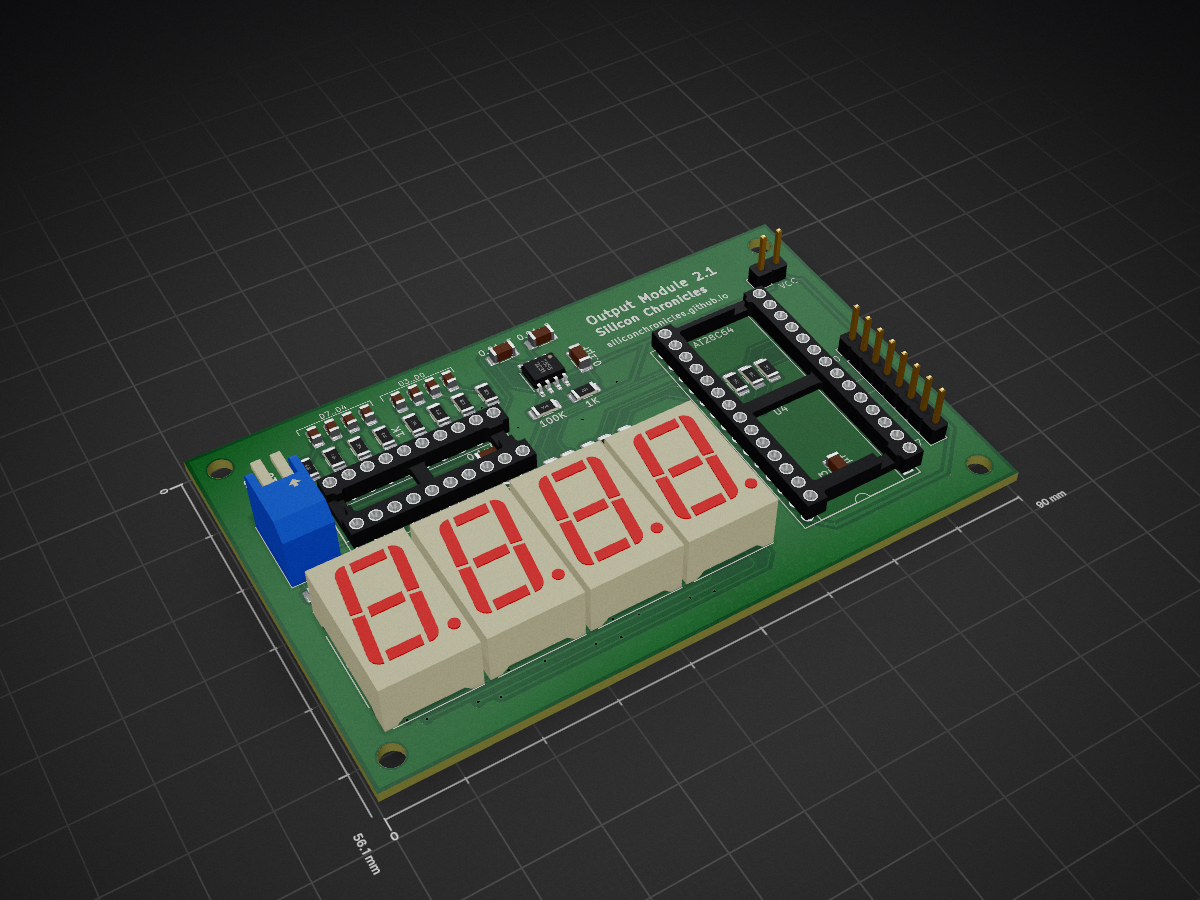
 siliconchronicles/output-module
A module to display 8-bit numbers
Output pal is an open-source printed circuit board by siliconchronicles, from the siliconchronicles/output-module repository on GitHub. It is a 2-layer board of 90 × 56.1 mm with 47 parts on 58 nets, routed with 381 tracks and 54 vias.
It is built around the HDSP-7503. Its parts include 20 resistors, 8 diodes, 7 ICs, 5 capacitors and 2 connectors. It belongs with the retro computing and games and lEDs and displays boards and the FPGA and CPLD boards of this library.
This is a description of a display for showing values of an 8-bit signal. This is useful for building and debugging breadboard digital circuits working with digital numbers.
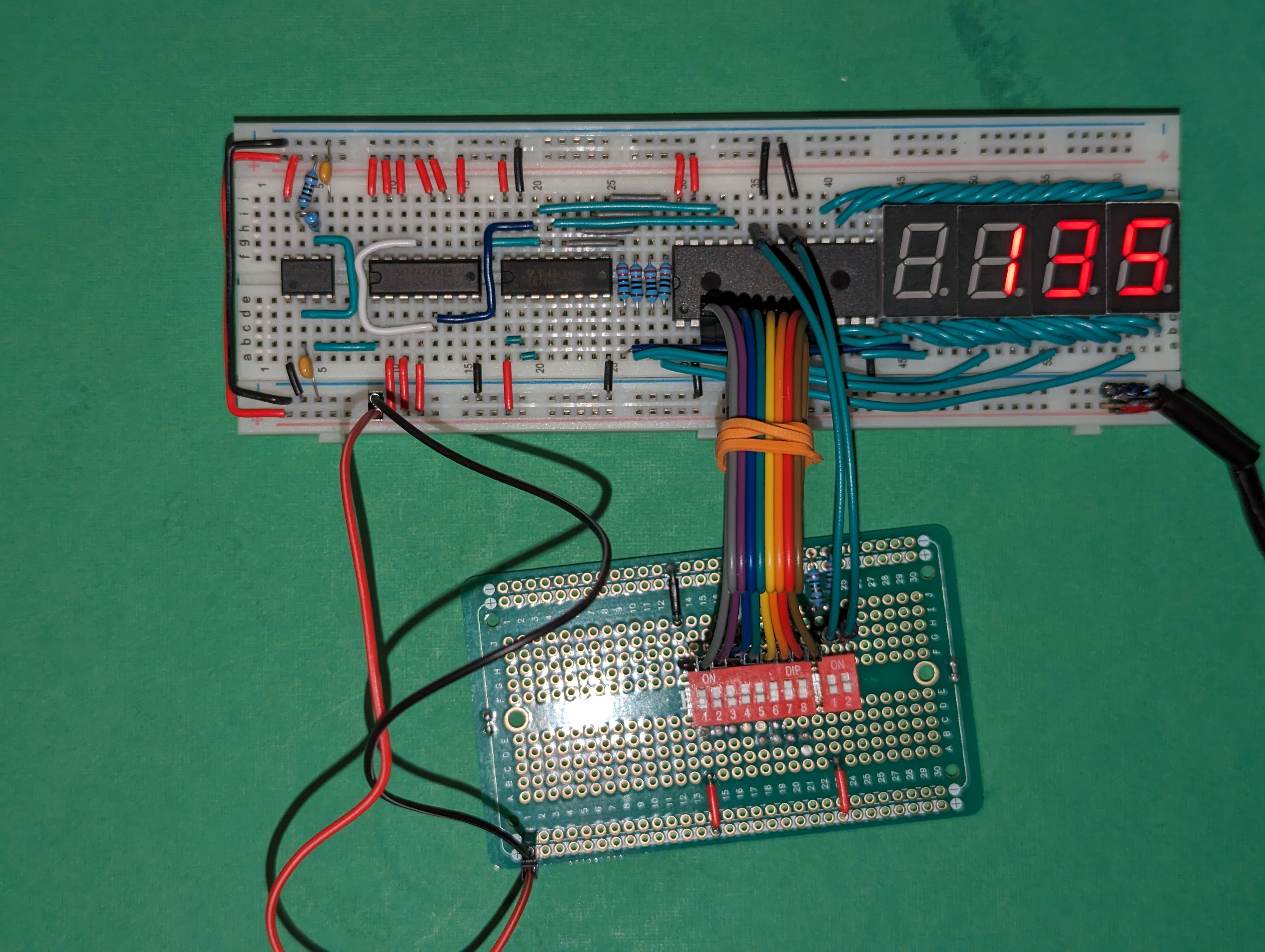
It's main features are:
It's inspired in Ben Eater's output register, but this is just the display (it does not contain register functionality). I decided to keep it as a separate unit that I can attach to any register to debug.

All ICs should be in DIP package if you're building in breadboards.
You can also choose TTL compatible components (LS or HCT families for the 74 series, and NE555 for the timer IC). As long as you're consistent, it's the same; all external inputs come into the EEPROM, which accepts both TTL and CMOS inputs.
The ROM image is generated by a Python script. I tried to make it easy to change. I'm also providing a pre-built ROM file if you want to use mine unchanged.
You will need an EEPROM programmer to write the ROM. The image generated only uses the lower 4KB (leaving the other 4KB unused). It would be possible to add other modes there if desired.
The Config section has a few settings that you can fiddle with; FONT is something you
can change without changing the circuit if you want to provide different selection of
segments or representable values. ROM_LAYOUT is used to customize the mapping of
segment to ROM pins; this has been configured for my breadboard layout so that the wires
from ROM to the segment stay in the same side of the breadboard and are tidier.
The generate_text() should produce the text representation for an 8-bit value in the
selected mode. shuffle() takes care of adjusting the bits described in the font to the
output pin layout selected.
If you set an invalid mode, the display should show ---- (four dashes).
| Qty | Value | Footprint | References |
|---|---|---|---|
| 18 | 1K | Resistor_SMD:R_1206_3216Metric_Pad1.30x1.75mm_HandSolder | R1, R3, R4, R5, R6, R7, R10, R11, R12, R13, R14, R15, R16, R17, R18, R19 +2 |
| 8 | LED | Capacitor_SMD:C_0805_2012Metric_Pad1.18x1.45mm_HandSolder | D1, D2, D3, D4, D5, D6, D7, D8 |
| 4 | HDSP-7503 | footprint-library:7SegmentLED_generic | U5, U6, U7, U8 |
| 3 | 0.1µF | Capacitor_SMD:C_1206_3216Metric_Pad1.33x1.80mm_HandSolder | C3, C4, C5 |
| 2 | 0.01µF | Capacitor_SMD:C_1206_3216Metric_Pad1.33x1.80mm_HandSolder | C1, C2 |
| 1 | 100K | Resistor_SMD:R_1206_3216Metric_Pad1.30x1.75mm_HandSolder | R2 |
| 1 | 1K | Resistor_SMD:R_1206_3216Metric | R20 |
| 1 | 7555 | Package_SO:SOIC-8_3.9x4.9mm_P1.27mm | U1 |
| 1 | AT28C64 | Package_DIP:DIP-28_W15.24mm_Socket | U4 |
| 1 | ATF16V8 | Package_DIP:DIP-20_W7.62mm_Socket | U9 |
| 1 | Conn_01x02_Pin | Connector_PinHeader_2.54mm:PinHeader_1x02_P2.54mm_Vertical | J3 |
| 1 | Conn_01x08_Pin | Connector_PinHeader_2.54mm:PinHeader_1x08_P2.54mm_Vertical | J1 |
| 1 | SW_DIP_x02 | Button_Switch_THT:SW_DIP_SPSTx02_Piano_10.8x6.64mm_W7.62mm_P2.54mm | SW1 |
The 43 most common of 47 parts.
It measures 90 × 56.1 mm and has 2 copper layers, 1.6 mm thick.
47 parts, built around the HDSP-7503. The full list of its parts is on this page, with links to each part's symbol and footprint where PCBKit's library has them.
From the siliconchronicles/output-module repository on GitHub, at the commit this page was made from: the board is schematic/output-pal/output-pal.kicad_pcb and its schematic schematic/output-pal/output-pal.kicad_sch. PCBKit opens the board in the browser, with nothing to install.
Its repository states no licence, so its author keeps all rights: ask siliconchronicles before reusing the design.

adhyayan15/BCD_Decade_Counter
Designed a custom KiCad PCB for a BCD decade counter, transitioning a verified breadboard prototype into a manufacturable circuit.


Roshan-khatri78/Electronics-Projects-KiCad-
A collection of my KiCad projects and PCB designs. These projects reflect my learning journey in electronics and PCB design.


