2 layers252.9 × 77.6 mm

 shanna/pla_nck32
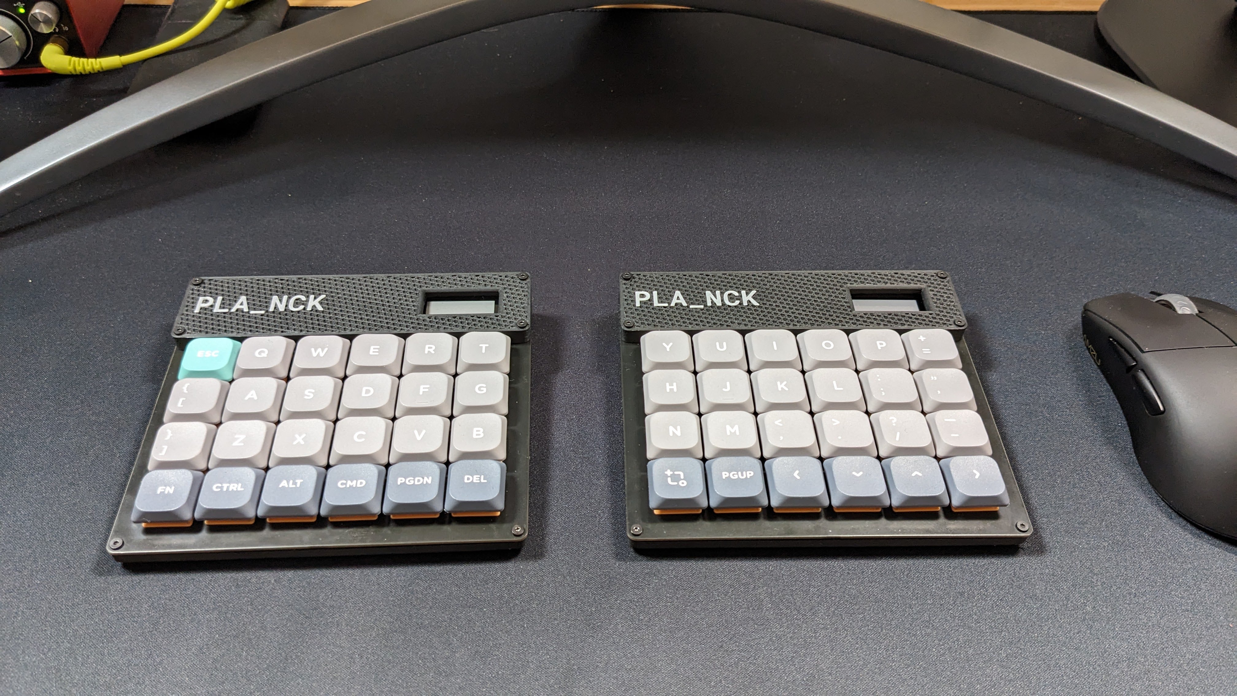
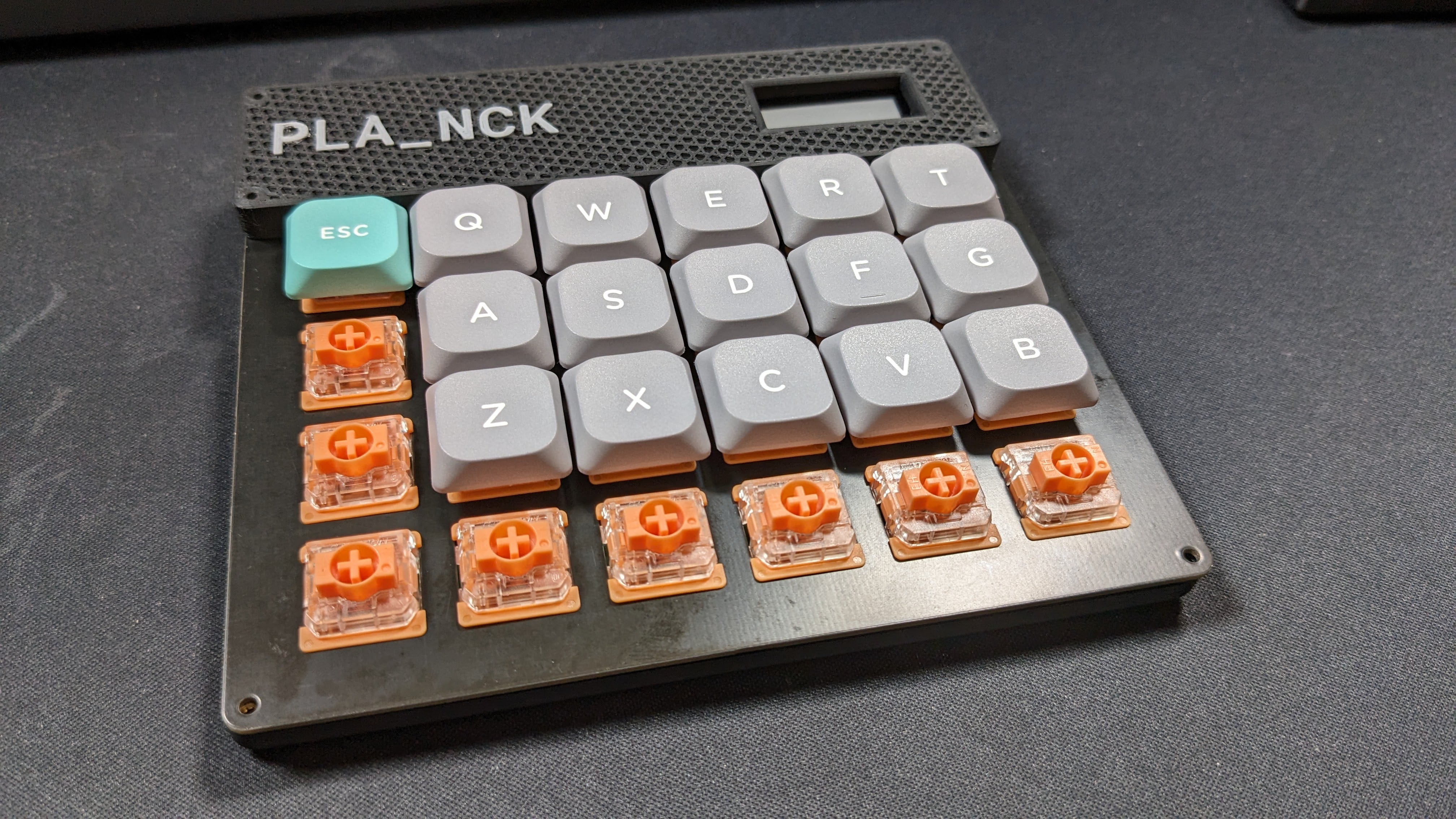
A low profile split keyboard I built using Gateron KS-33 low profile switches.
Pla nck is an open-source printed circuit board by shanna, from the shanna/pla_nck repository on GitHub. It is a 2-layer board of 118.7 × 103.8 mm with 58 parts on 48 nets, routed with 343 tracks and 31 vias.
Its parts include 24 diodes, 24 switches and 1 IC. It belongs with the nRF52 and nRF5x boards of this library.
A low profile split keyboard I built using Gateron KS-33 low profile switches.
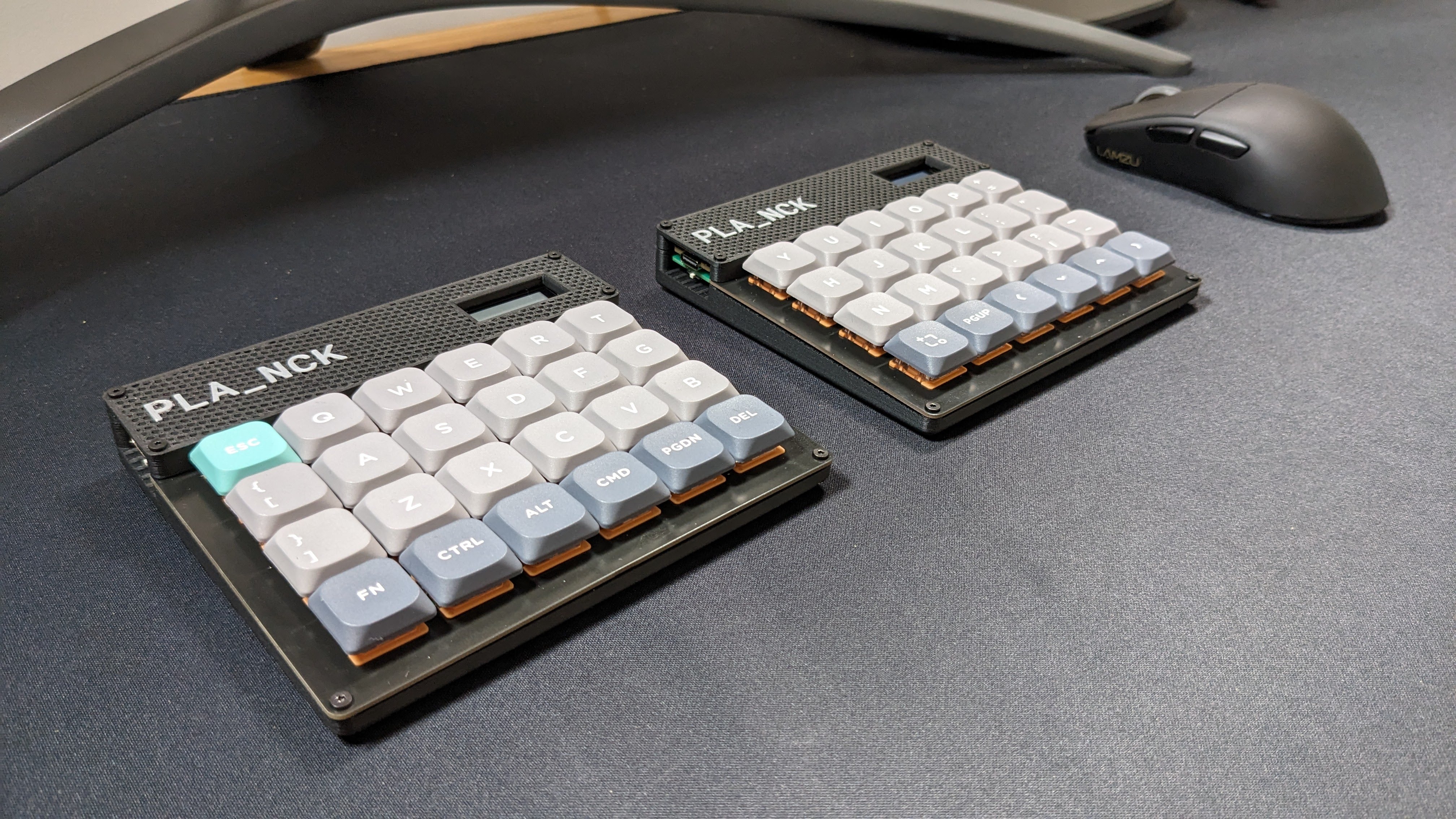
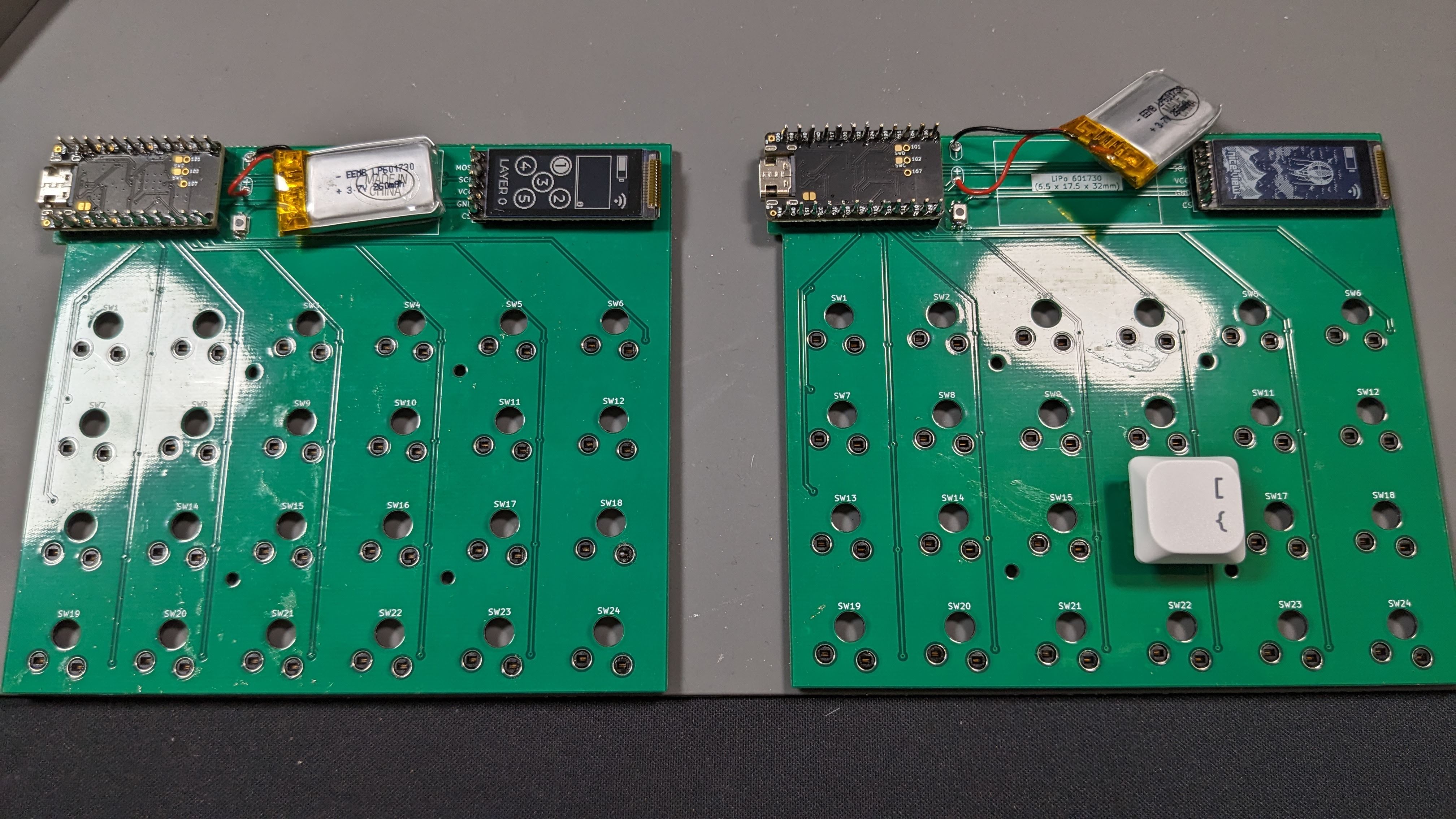
I had assembled a Ferris Sweep previously but I hated the Kailh Low Profile Choc Switches but but wanted something low profile. Sincve I couldn't find anything at the time I decided to learn KiCad and Fusion360 to create my own design.
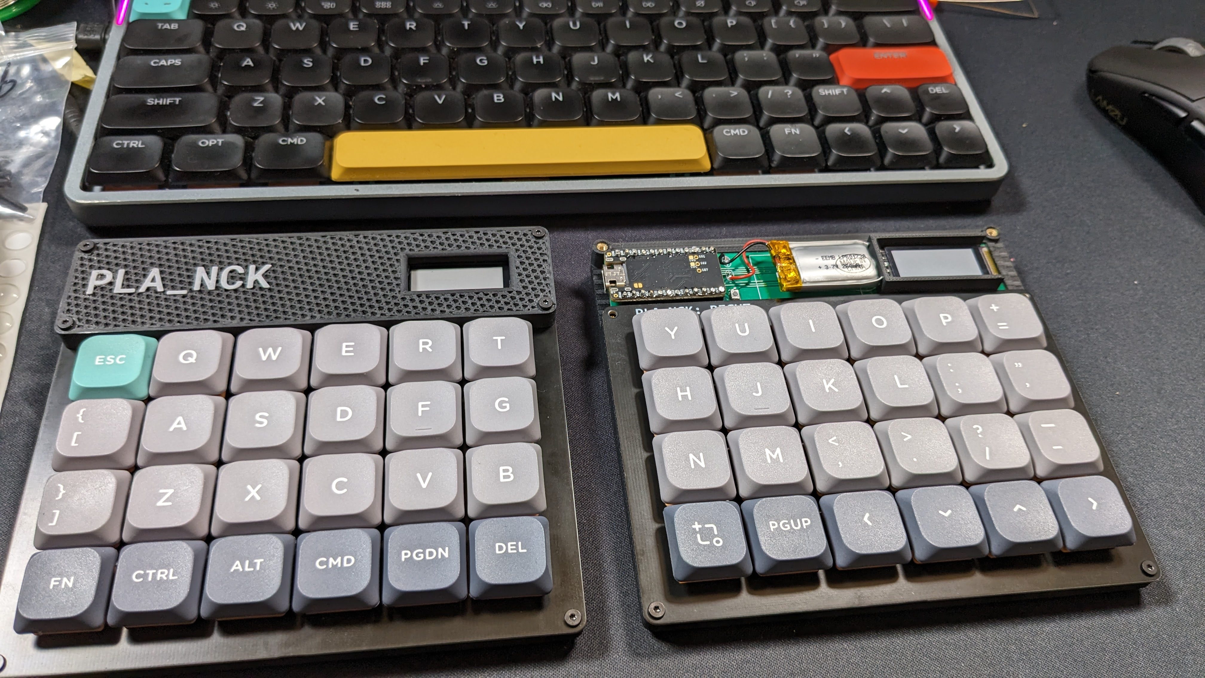
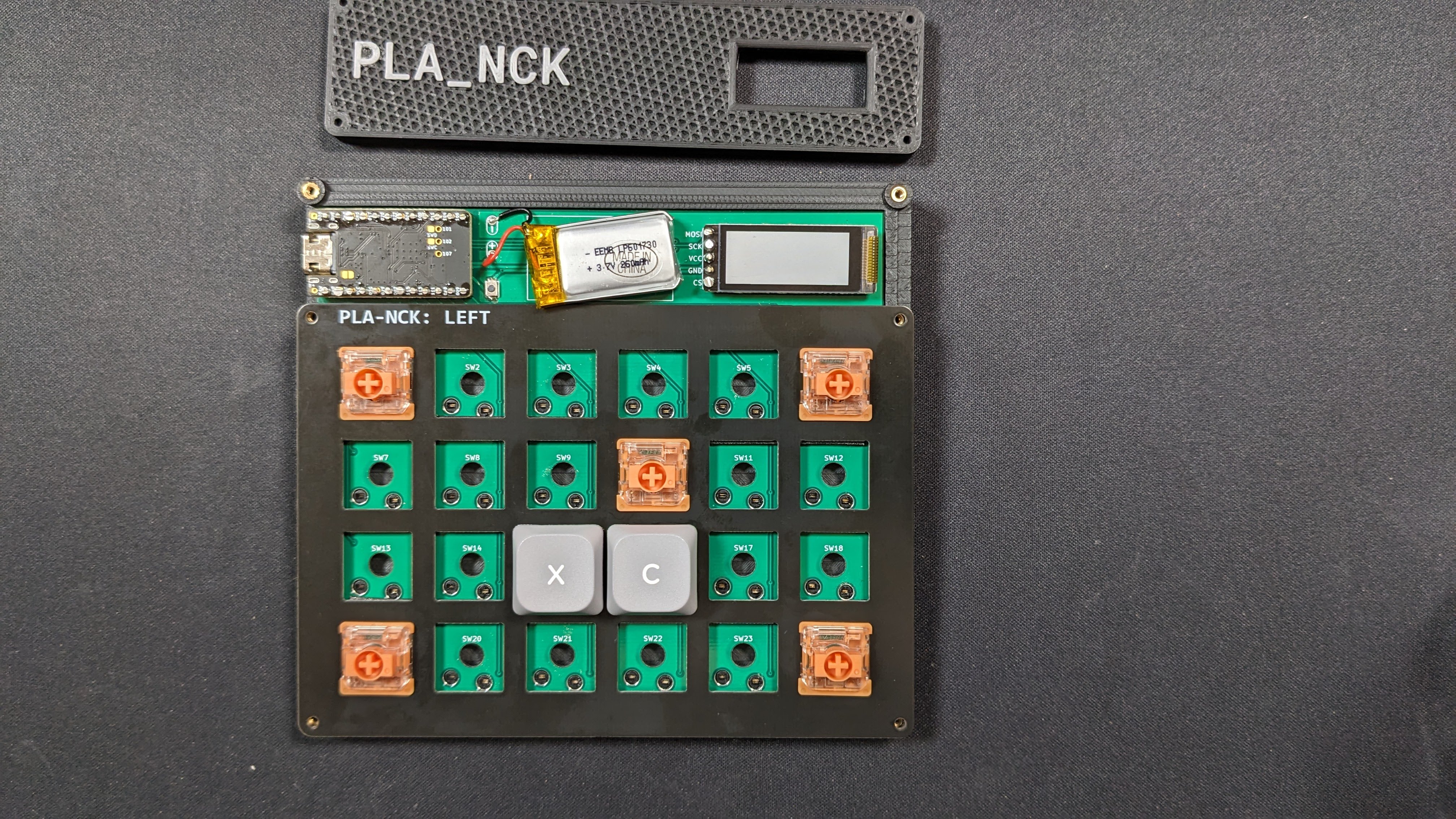
I've called it the PLA_NCK because my original intention was to create a split ZSA Planck EZ (discontinued) since it has probably been my favourite layout to date. I justed wanted a split, bluetooth and low profile version with Gateron KS-33 switches after using the NuPhy Air60 with Daisy Gateron colaboration switches. I couldn't quite fit the controller under the keys while keeping it low so I gave up and added the nice view as well for this version so my homage to the original Planck is a bit shit. I might attempt it again with without a pre-made controller when my KiCad skills improve so I can ditch the display and make it closer to the split plank low profile vision I started with.
The AliExpress stuff will be hit and miss.
Everything you need is included in this repo I think.
Version 1 I tried to add mass by printing the case with 60% infill in PLA and hoped it would improve the sound. It was better than nothing but a bit too loud for the office.
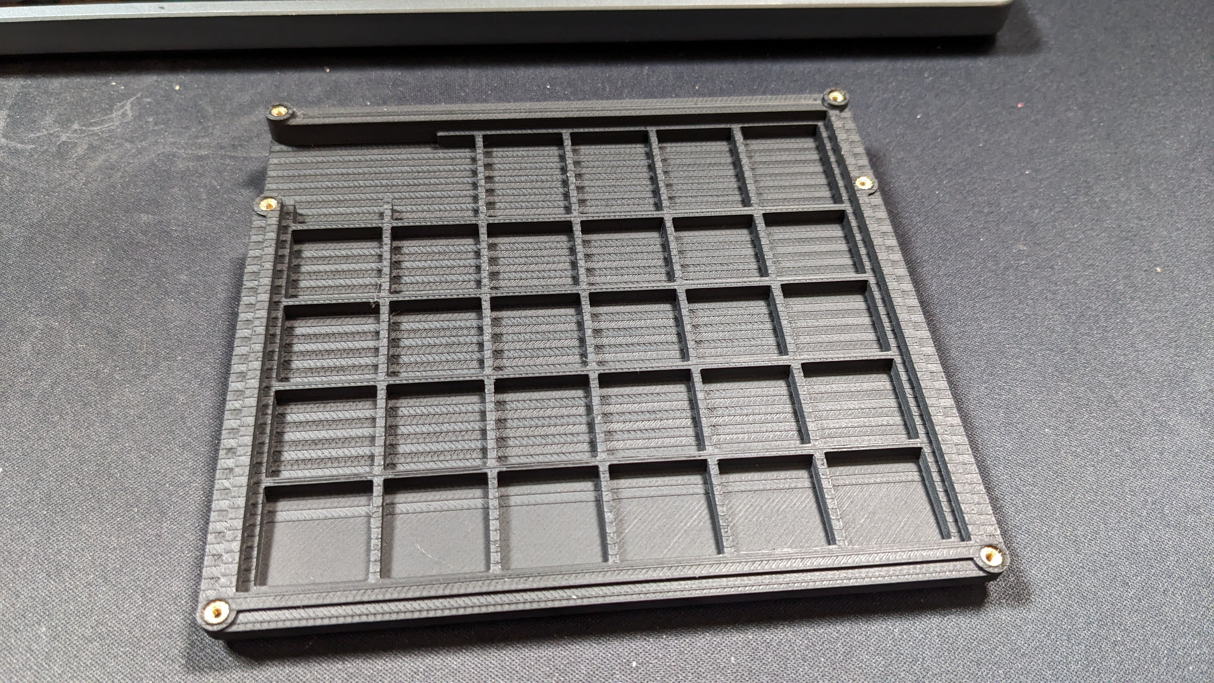
Version 2 I've simplified the PLA case and printed a mount in TPU that sits between the PCB and plate and bolts directly to the case. Keyboard switch sounds is subjective (some blue use MX blues) but this removed a lot of the high frequency plastic "ping" I wasn't happy with. There is still room for improvement if you have any ideas. I've been experimenting with different foams and TPU inserts in the case to remove more of the high frequencies because I want more "thock" and less "clack".
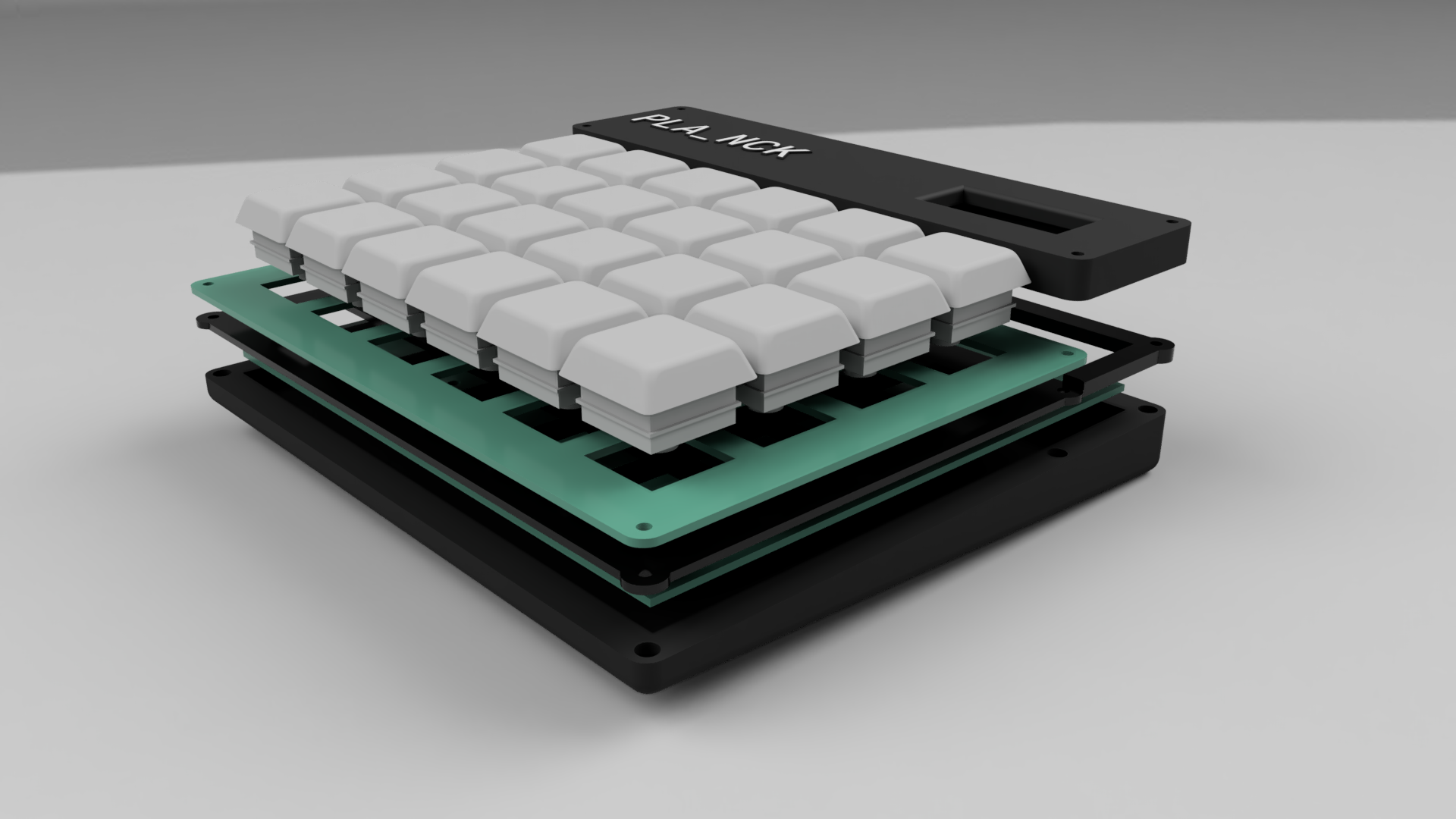
I'm running ZMK on my nice!nano's. The config/ directory contains all the ZMK config you need to match the pin-out and diode direction along with my current key map (which sucks but is a starting point).
The makefile expects nix to be installed and runs 'act' the local github actions runner to test the ZMK github actions. It has nowhere to write artifacts out to but is handy for checking your configuration files are valid before uploading them to github.
Tolerances are tight, too tight in places, depending on the PCB manufacturer and 3D printer setup and material you print in. I used PLA but I still struggled with shrinkage so tried to hide it with some shadow lines.
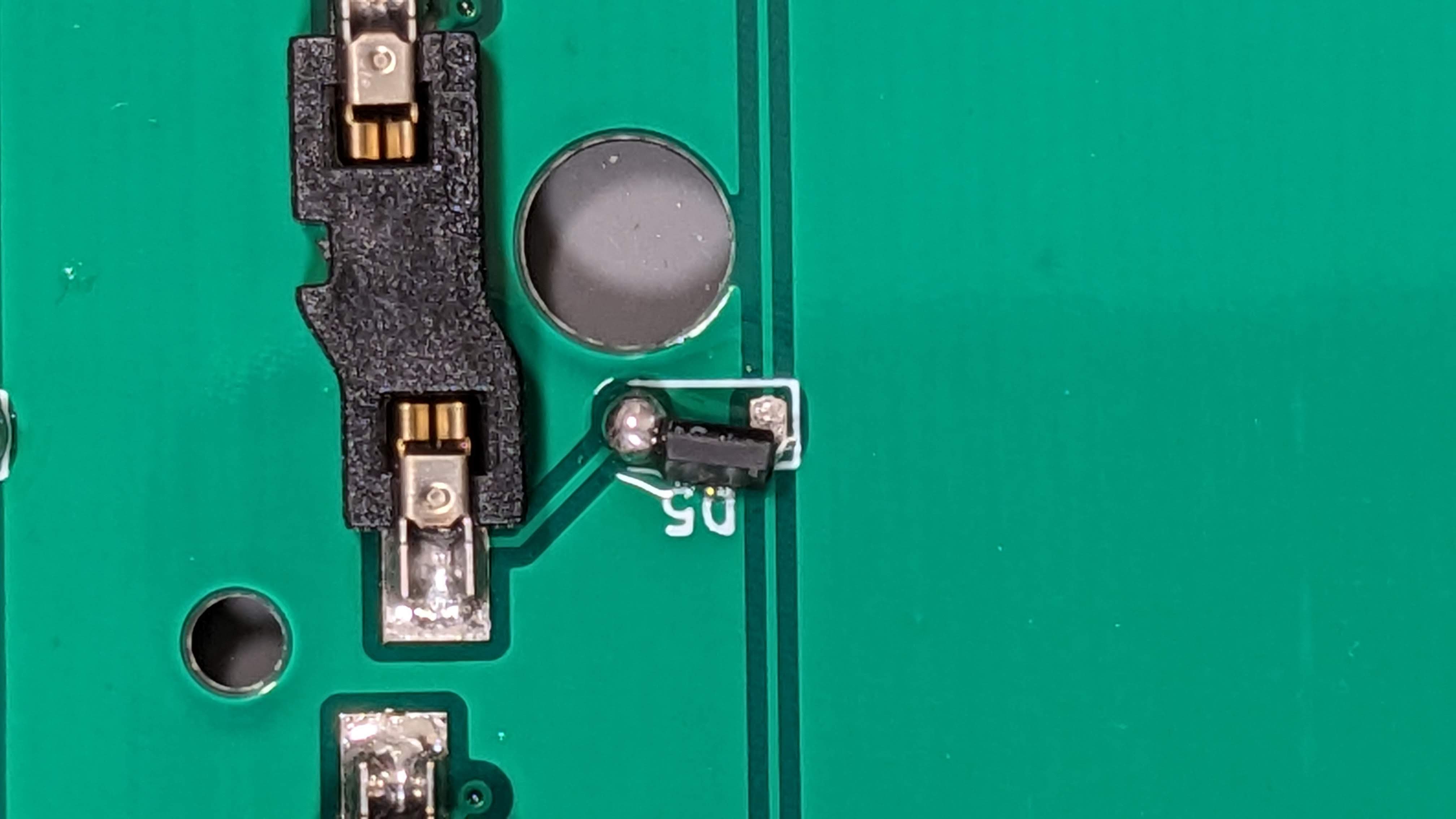
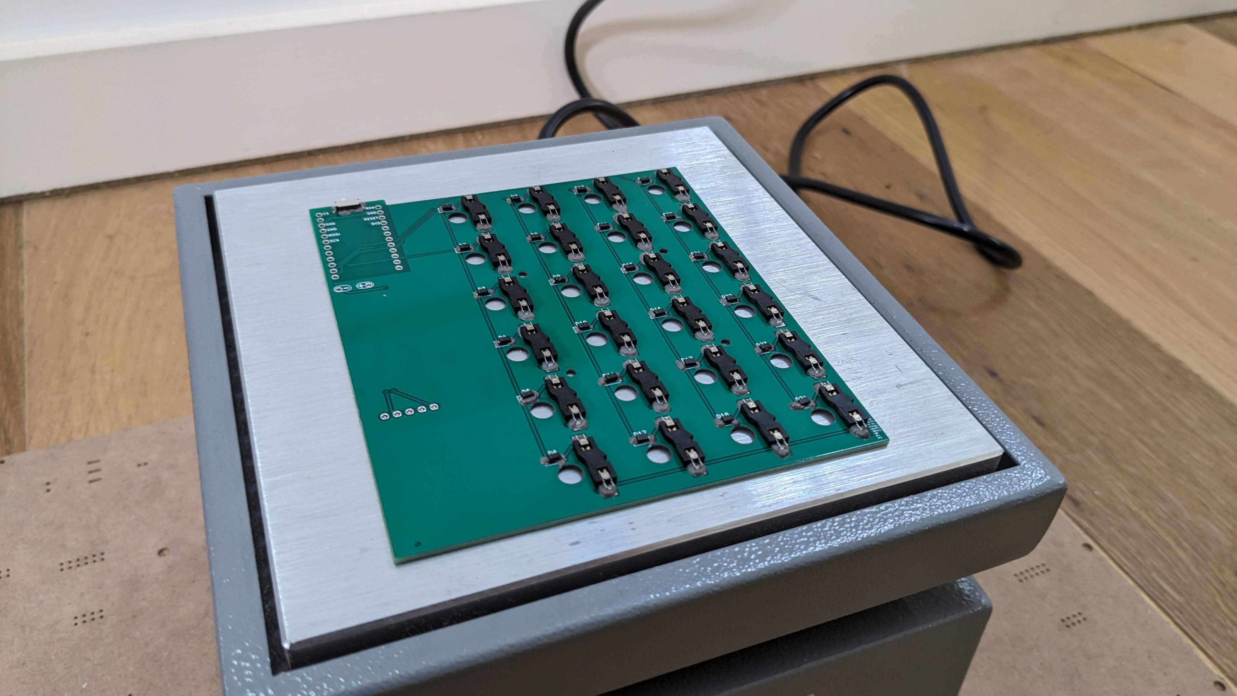
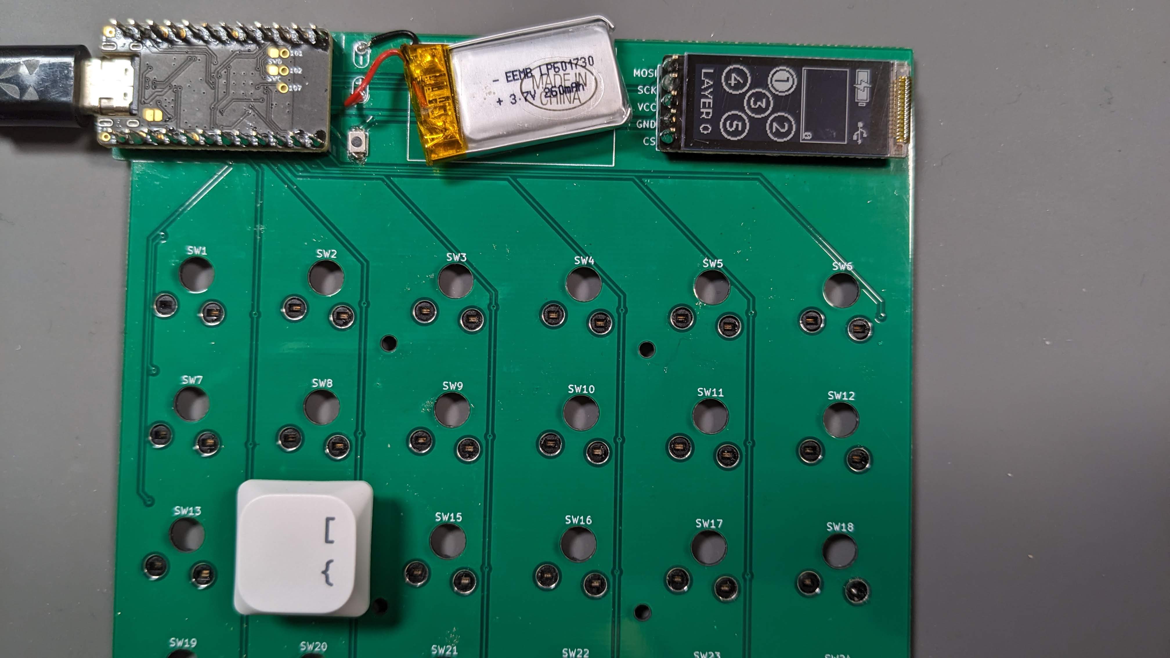
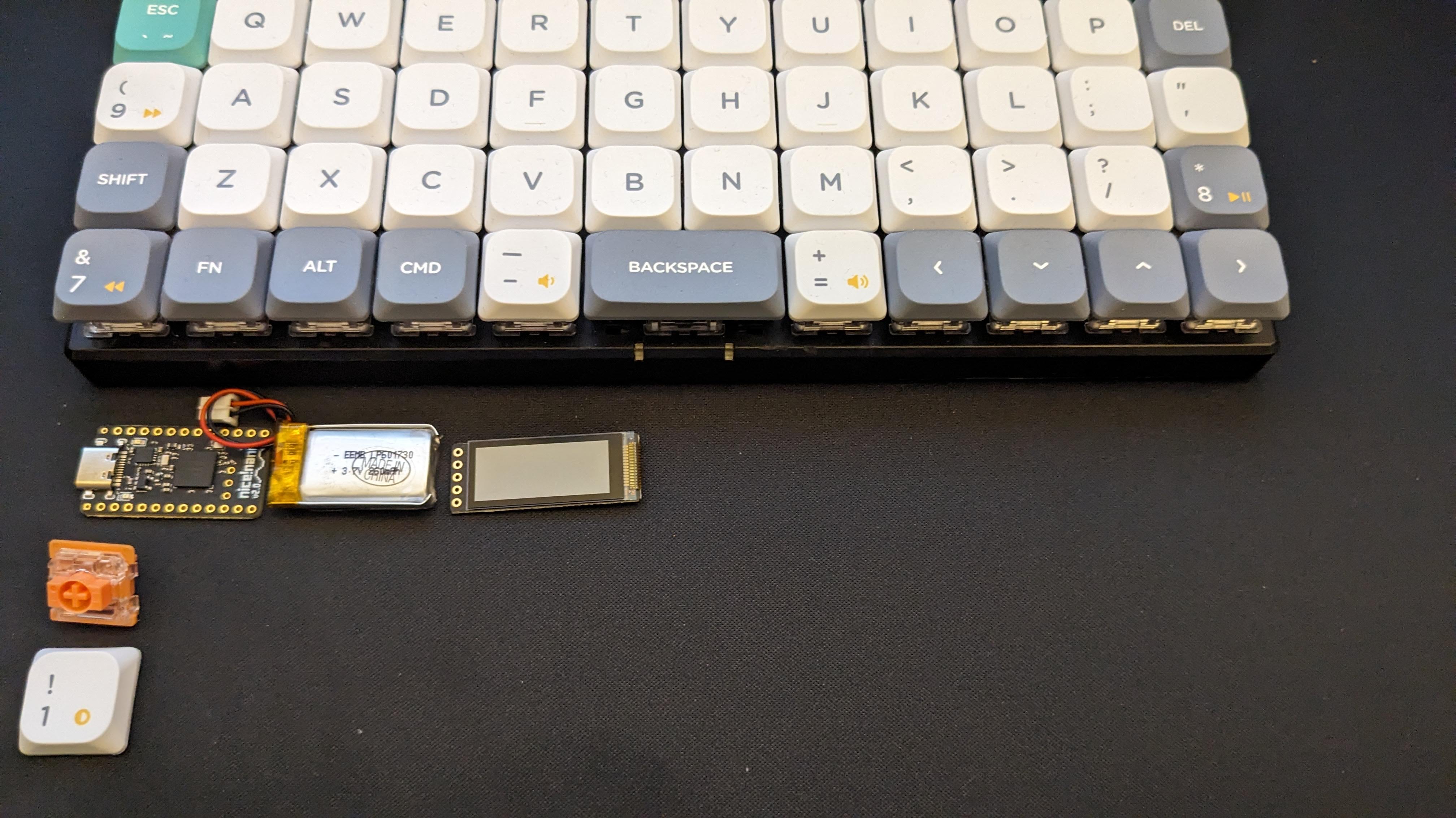
| Qty | Value | Footprint | References |
|---|---|---|---|
| 24 | Gateron KS-27 | lib:SW_Gateron_KS27_NO_LED | SW1, SW2, SW10, SW11, SW12, SW13, SW14, SW15, SW16, SW17, SW18, SW19, SW20, SW21, SW22, SW23 +8 |
| 24 | diode | Diode_SMD:D_SOD-123 | D1, D2, D10, D11, D12, D13, D14, D15, D16, D17, D18, D19, D20, D21, D22, D23 +8 |
| 4 | PlateSupport | MountingHole:MountingHole_2.2mm_M2 | HPS1, HPS2, HPS3, HPS4 |
| 2 | MountingHole_Pad | lib:1pin_battery_v2 | Bat+1, BatGND1 |
| 1 | RESET | lib:SW_RESET | RSW1 |
| 1 | SW_SPDT | lib:smt-slider-switch | SW_POWER1 |
| 1 | nice!nano | lib:nice_nano | U1 |
| 1 | nice!view | lib:nice_view | Display1 |


zynthian/zynthian-hw
Zynthian hardware stuff: PCBs, schemes, parts specifications, pin assignment, ...


Hack-a-Day/2025-Communicator_Badge
The 2025 Hackaday Supercon RF Communicator Badge


rheslip/2HPico-Eurorack-Module-Hardware
2HP Eurorack module based on Raspberry Pi Pico 2

mck1117/wideband
The firmware/boards directory contains configuration for each board this firmware supports.
It measures 118.7 × 103.8 mm and has 2 copper layers, 1.2 mm thick.
58 parts. The full list of its parts is on this page, with links to each part's symbol and footprint where PCBKit's library has them.
From the shanna/pla_nck repository on GitHub, at the commit this page was made from: the board is pcb/pla_nck.kicad_pcb and its schematic pcb/pla_nck.kicad_sch. PCBKit opens the board in the browser, with nothing to install.
Its repository states no licence, so its author keeps all rights: ask shanna before reusing the design.