
2 layers231.1 × 106.7 mm

 shack/knoepfchen2
A small PCB with debounced buttons and switch to put on breadboards
Knoepfchen is an open-source printed circuit board by shack, from the shack/knoepfchen repository on GitHub, published under the MIT licence. It is a 2-layer board of 30.7 × 34.9 mm with 16 parts on 19 nets, routed with 84 tracks and 0 vias.
It is built around the 74LS14PC. Its parts include 5 resistors, 4 capacitors, 3 connectors, 2 ICs and 2 switches.
The unpronounceable PCB!
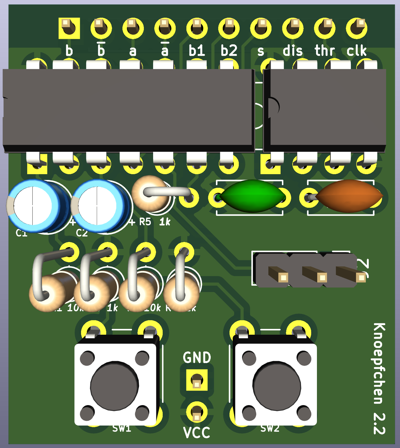
A small PCB with two debounced buttons, a debounced SPDT switch, and a 555 in astable configuration.
When experimenting with logic circuits, one often needs a switch or a button or a clock. However, putting small debounce circuits on the breadboard over and over again is tedious. Knoepfchen is a small PCB that you can just put on your breadboard and get two debounced buttons, a debounced switch, a 555 in astable mode, a two inverters with all relevant connectors available.
Knoepfchen has to rows of connectors: The lower ones connect to the power rails of the breadboard. The upper row can be plugged into the upper half of the breadboard and exposes all relevant connectors. These are from left to right:
| Number | Label | I/O | Description |
|---|---|---|---|
| 1 | a | I | Input to an 74HCT14 inverter |
| 2 | ~a | O | Negation of a (output of inverter) |
| 3 | b | I | Input to an 74HCT14 inverter |
| 4 | ~b | O | Negation of b (output of inverter) |
| 5 | b1 | O | Debounced button 1 (active high) |
| 6 | b2 | O | Debounced button 2 (active high) |
| 7 | s | O | Position 1 of debounced SPDT switch |
| 8 | DIS | - | Pin 7 of 555 |
| 9 | THR | - | Pin 6 of 555 |
| 10 | CLK | O | Pin 3 of 555 |
Here, a brief summary of two standard configurations to get a clock signal out of the 555.
The frequency is then $\frac 1{\ln 2\cdot(R_1+2R_2)\cdot C}$ and the duty cycle is $\frac {R_1+R_2}{R_1+2R_2}$
The frequency is then $\frac 1{2\ln 2\cdot RC}$
More details on both configurations and more can be found for example here.
| Qty | Value | Footprint | References |
|---|---|---|---|
| 3 | 1k | Resistor_THT:R_Axial_DIN0207_L6.3mm_D2.5mm_P2.54mm_Vertical | R3, R4, R5 |
| 2 | 100nF | Capacitor_THT:C_Disc_D5.0mm_W2.5mm_P5.00mm | C4, C5 |
| 2 | 10k | Resistor_THT:R_Axial_DIN0207_L6.3mm_D2.5mm_P2.54mm_Vertical | R1, R2 |
| 2 | 1µF | Capacitor_THT:CP_Radial_D4.0mm_P1.50mm | C1, C2 |
| 2 | SW_SPST | Button_Switch_THT:SW_PUSH_6mm | SW1, SW2 |
| 1 | 74LS14 | Package_DIP:DIP-14_W7.62mm | U2 |
| 1 | Conn_01x02_Pin | Connector_PinHeader_2.54mm:PinHeader_1x02_P2.54mm_Vertical | J1 |
| 1 | Conn_01x03_Pin | Connector_PinHeader_2.54mm:PinHeader_1x03_P2.54mm_Vertical | J2 |
| 1 | Conn_01x10_Pin | Connector_PinHeader_2.54mm:PinHeader_1x10_P2.54mm_Vertical | J3 |
| 1 | TLC555xP | Package_DIP:DIP-8_W7.62mm | U1 |
It measures 30.7 × 34.9 mm and has 2 copper layers, 1.6 mm thick.
16 parts, built around the 74LS14PC. The full list of its parts is on this page, with links to each part's symbol and footprint where PCBKit's library has them.
From the shack/knoepfchen repository on GitHub, at the commit this page was made from: the board is knoepfchen.kicad_pcb and its schematic knoepfchen.kicad_sch. PCBKit opens the board in the browser, with nothing to install.
Its repository publishes it under the MIT licence: you may reuse it on that licence's terms (keep the author's notice, and for a copyleft licence share your changes alike).

schlae/comix-35
The COMIX-35 is an improved clone of the COMX-35 1802 home computer

monotech/NuXT
MicroATX Turbo XT Motherboard, with VGA, Floppy, CF, Serial


skiselev/zeta_sbc
Zeta SBC is an Zilog Z80 based single board computer. It is inspired by Ampro Little Board Z80 and N8VEM project. Zeta SBC is software compatible with RomWBW Firmware

tebl/C64-Lumafix
An easier to solder version of the Lumafix board, components spaced out a bit more to make things easier on the beginner (mostly meaning me).

