4 layers25.8 × 62.7 mm
PulseboardS3
I-s-h-a-n-C/PulseboardS3
This is an ESP32 S3 Devboard, designed to be used in conjunction with EMGs and EKGs. As with all ESP32S3 Devboards, it has WiFi and Bluetooth capibilities.
31 parts

 SendhanS/ESP32-Sen1
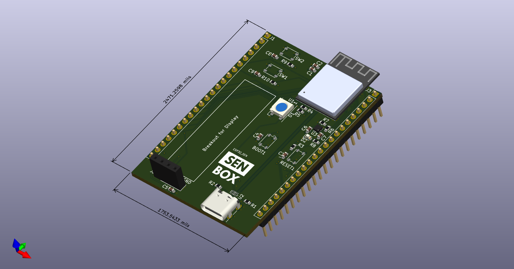
A compact ESP32-S3-MINI-1-N8 development board with USB-C (ESD protected), a 4-layer PCB stack-up (signal / GND / power / signal), and 3.3 V regulation using the TLV75801. Includes GPIO buttons, a WS2812B status LED, and space for an onboard I²C OLED breakout.
ESP32-Sen is an open-source printed circuit board by SendhanS, from the SendhanS/ESP32-Sen repository on GitHub, published under the CC0-1.0 licence. It is a 4-layer board of 44.5 × 62.8 mm with 33 parts on 55 nets, routed with 538 tracks and 143 vias.
It is built around the ESP32-S3-MINI-1-N8, ESD7104MUTAG and TLV75801PDRV, with the WS2812B among its other parts. Its parts include 10 resistors, 9 capacitors, 3 ICs, 3 connectors and 2 diodes. It belongs with the ESP32 boards of this library.


A compact ESP32-S3-MINI-1-N8 development board with USB-C (ESD protected), a 4-layer PCB stack-up (signal / GND / power / signal), and 3.3 V regulation using the TLV75801. Includes GPIO buttons, a WS2812B status LED, and space for an onboard I²C OLED breakout. The board is intended for learning, experimentation, and portfolio demonstration of embedded systems and PCB design practices. Status: Not yet tested. The design is functional in theory but may require revisions and improvements after bring-up.
Overview
This board provides a clean ESP32-S3 core with USB-C connectivity, proper ESD protection, a structured 4-layer PCB stack-up, and expansion options for basic UI and peripherals. The goal was to move beyond simple 2-layer hobby boards and design something closer to real-world embedded hardware.
Key Features
ESP32-S3-MINI-1-N8 module
USB-C connector (USB4105)
Differential USB D+ / D− routing
ESD protection using D3V3XA4B10LP TVS diodes
TLV75801 linear regulator (5 V USB → 3.3 V)
4-layer PCB stack-up:
Top: Signal + components
Inner 1: Solid GND plane
Inner 2: Power plane (3.3 V)
Bottom: Signal routing
WS2812B RGB status LED
BOOT and RESET buttons
Two additional GPIO buttons (GPIO4, GPIO5)
Power Architecture
Primary power input via USB-C (5 V)
Onboard TLV75801 LDO generates 3.3 V for ESP32 and peripherals
3.3 V rail is exposed on headers for external devices
Design allows future extension for alternative power input with minor modifications
I²C header and reserved space for a 0.91" OLED display module
GPIO headers for expansion
USB Design Notes
USB D+ and D− routed as a differential pair
Length-matched and impedance-aware routing
ESD protection placed close to the USB connector
Intended for USB device mode (programming and serial communication)
I²C and Display Support
Dedicated I²C header (3.3 V logic)
PCB space reserved for a common 0.91" 128×32 I²C OLED module
Display is optional and not populated by default
Known Limitations / Future Improvements
Board has not been fabricated or tested yet
No battery power or charging circuit
No current measurement or power monitoring
Firmware bring-up examples not included yet
OLED mounting footprint may need adjustment depending on module vendor
| Qty | Value | Footprint | References |
|---|---|---|---|
| 6 | 0.1uF | Capacitor_SMD:C_0603_1608Metric | C1, C3, C4, C5, C8, C9 |
| 5 | 10k | Resistor_SMD:R_0603_1608Metric | R3, R4, R5, R9, R10 |
| 3 | 10uF | Capacitor_SMD:C_0603_1608Metric | C2, C6, C7 |
| 3 | 5.1k | Resistor_SMD:R_0603_1608Metric | R1, R2, R8 |
| 2 | SW_MEC_5E | Button_Switch_SMD:SW_SPST_PTS810 | SW1, SW2 |
| 2 | ~ | Button_Switch_SMD:SW_SPST_PTS810 | BOOT1, RESET1 |
| 2 | ~ | Connector_PinHeader_2.54mm:PinHeader_1x22_P2.54mm_Vertical | J1, J3 |
| 1 | 1M | Resistor_SMD:R_0603_1608Metric | R6 |
| 1 | 200k | Resistor_SMD:R_0603_1608Metric | R7 |
| 1 | ESD7104MUTAG | Package_DFN_QFN:Diodes_UDFN-10_1.0x2.5mm_P0.5mm | U2 |
| 1 | ESP32-S3-MINI-1-N8 | ESP32-S3-MINI-1-N8:XCVR_ESP32-S3-MINI-1-N8 | U1 |
| 1 | I2C Port | Connector_PinSocket_2.54mm:PinSocket_1x04_P2.54mm_Vertical | J2 |
| 1 | LED | LED_SMD:LED_0603_1608Metric | D2 |
| 1 | LOGO | LOGO | G*** |
| 1 | TLV75801PDRV | Package_SON:WSON-6-1EP_2x2mm_P0.65mm_EP1x1.6mm | U3 |
| 1 | USB_C_Receptacle_USB2.0 | Connector_USB:USB_C_Receptacle_GCT_USB4105-xx-A_16P_TopMnt_Horizontal | JUSB1 |
| 1 | WS2812B | LED_SMD:LED_WS2812B_PLCC4_5.0x5.0mm_P3.2mm | D1 |
It measures 44.5 × 62.8 mm and has 4 copper layers, 1.6 mm thick.
33 parts, built around the ESP32-S3-MINI-1-N8, ESD7104MUTAG, TLV75801PDRV and WS2812B. The full list of its parts is on this page, with links to each part's symbol and footprint where PCBKit's library has them.
From the SendhanS/ESP32-Sen repository on GitHub, at the commit this page was made from: the board is ESP32_Sen.kicad_pcb and its schematic ESP32_Sen.kicad_sch. PCBKit opens the board in the browser, with nothing to install.
Its repository publishes it under the CC0-1.0 licence: you may reuse it on that licence's terms (keep the author's notice, and for a copyleft licence share your changes alike).
I-s-h-a-n-C/PulseboardS3
This is an ESP32 S3 Devboard, designed to be used in conjunction with EMGs and EKGs. As with all ESP32S3 Devboards, it has WiFi and Bluetooth capibilities.


cs99x/GasMonitorLoRaCloud
This project is a mobile and embedded application for a university course called "Mobile and Embedded Development".

greigs/OpenBrickGB
Functional / Playable Lego Game Boy Electronics - PCB Design Files

BirryGit/Battery-Powered-Meshtastic-Board
I want to learn how to make PCBs, and this seemed like a good idea. I originally was following the Stasis tutorial, but veered away from it significantly. I want to get into meshtastic, so this is awesome :)