


2 layers119.4 × 119.4 mm
Esp32-pool controller
niko34/esp32-pool-controller
Contrôleur automatique de piscine ESP32 avec gestion pH, ORP, température, filtration, éclairage, app web locale, MQTT (HomeAssistant auto-discovery), API
93 partsMIT

 seesharp15/cloudline-fan-controller
The controller on a printed circuit board instead of perfboard:
Cloudline controller is an open-source printed circuit board by seesharp15, from the seesharp15/cloudline-fan-controller repository on GitHub. It is a 2-layer board of 100 × 75 mm with 28 parts on 20 nets, routed with 100 tracks and 0 vias.
It is built around the MCP1700-3302E/TT, BAT85 and P6KE13A. Its parts include 7 resistors, 5 capacitors, 4 diodes, 3 ICs and 3 connectors.


The controller on a printed circuit board instead of perfboard:
It carries every part in the schematic, plus a 4-way screw terminal for the fan cable and two pin headers for the OLED module.
This page covers everything about the board:
| Top (parts side) | Bottom copper (as seen from below) |
|---|---|
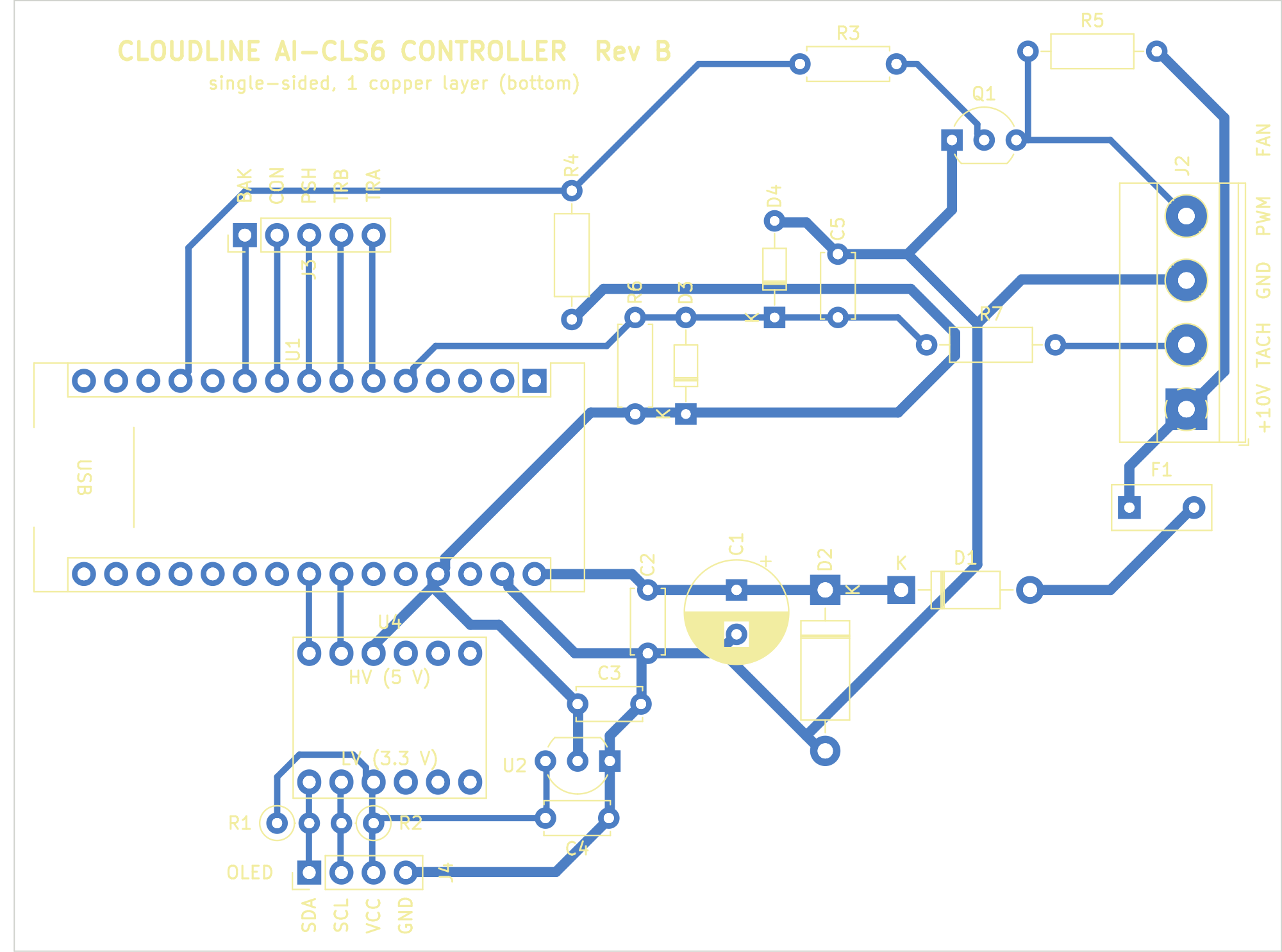 | 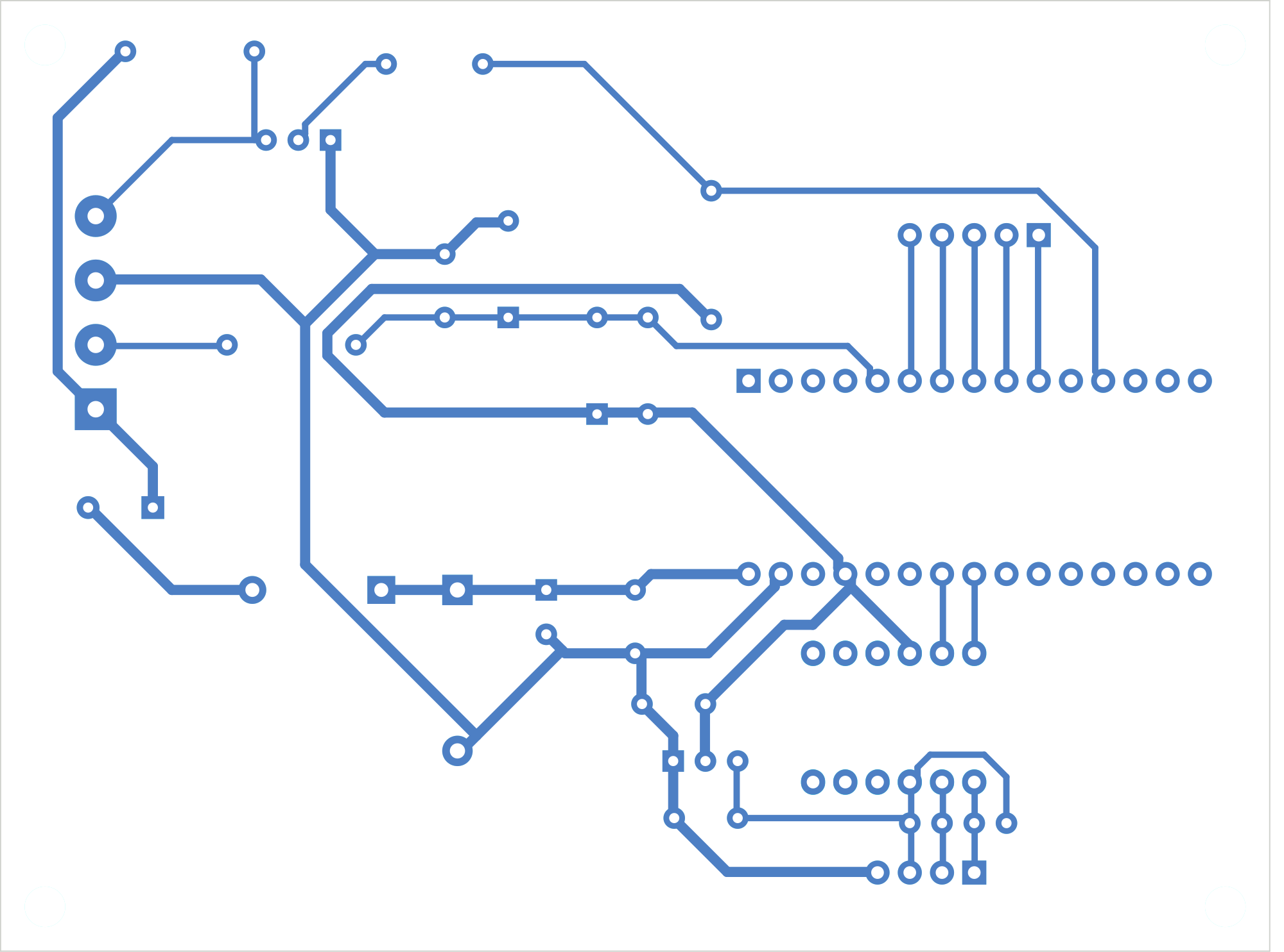 |
Status: designed and checked, not yet made. The files pass KiCad's design-rule check, an independent copper-connectivity check, an independent review, and the milling and EAGLE export checks below. No board has been built from them yet, and nothing has been opened in Fusion 360 or run on the machine. Build the first one expecting to find something.
| Route | Use | Sessions |
|---|---|---|
| A. Mill it on the Stepcraft M.1000 with Fusion 360 | Files in fusion/ | S0 → S18, all of them |
| B. Order it from a board house | Upload fab/cloudline_controller_RevB_gerbers_drill.zip, see Ordering | S0, S1, order, then S11 → S18 |
| C. Etch it at home by toner transfer | Print fab/bottom_copper_toner_transfer_1to1.pdf at 100 % | S0, S1, etch, drill by hand, then S11 → S18 |
To change the circuit or the layout, use Fusion Electronics (session S2).
The milling files in fusion/ and the Gerbers in fab/ are made from the
KiCad copy of the board. They don't change when you edit in Fusion. See
Which copy is master.
The milling files and the walkthrough are made for this setup:
| Machine | Stepcraft M.1000 with tool changer |
| Control software | UCCNC (Autodesk's UCCNC post in Fusion) |
| Spindle | Stepcraft DI 1000, 8 000–20 000 rpm |
| CAM | Fusion 360, commercial licence: one program with all tool changes, real rapids |
| Blank | FR-4; thickness is measured in S3; the copper weight doesn't matter (the cut works for 35 and 70 µm) |
| Workholding | Double-sided tape, Z touch plate, no height map |
| Tools (T1–T7) | T1 V-bit 30° with 0.1 mm tip · T2 0.8 mm drill · T3 1.0 · T4 1.2 · T5 1.3 · T6 3.2 · T7 2 mm 2-flute end mill |
Assumed and to confirm:
S4 says how to change any of these.
Board numbers that matter for milling:
Gaps: the smallest gap between copper of different nets is 0.64 mm. It sits between neighbouring 2.54 mm-pitch header pads, and no layout can make it larger. Tracks keep at least 0.69 mm from other copper. Copper is at least 3.15 mm from the board edge.
Isolation cut: two passes with the V-bit, 0.20 mm deep, 0.207 mm wide. That clears about 0.33 mm around every pad and track.
Holes: 99, all non-plated:
| Size | 0.75 | 0.80 | 1.00 | 1.10 | 1.20 | 1.30 | 3.20 (M3) |
|---|---|---|---|---|---|---|---|
| Count | 4 | 32 | 51 | 2 | 2 | 4 | 4 |
For milling (route A): fusion/
| File | What it is |
|---|---|
fusion/cloudline_pcb_MILL_copper_up.step | The model to machine, copper side up as it lies on the machine. It holds the FR-4 body with all holes, and one 0.035 mm copper body per net. The origin is the board's lower-left corner. Z = 0 is the underside; the copper top is at Z = 1.635. |
fusion/cloudline_pcb_MILL_copper_up.dxf | Same view in 2D, in mm. Layers: ISO_PASS1/ISO_PASS2 (isolation tool-centre paths), DRILL_* (one per hole size), OUTLINE, COPPER, FIDUCIAL |
fusion/cloudline_pcb_tools.json | Fusion tool library T1–T7, with feeds and speeds for the DI 1000 |
fusion/cloudline_pcb_TOPVIEW.step | The board seen from the parts side, for checks or an enclosure model. Not for machining. |
fusion/milling_report.txt, fusion/isolation_preview.png, fusion/mill_preview.png | Gaps, hole table and cut-width table, and pictures of the paths and copper |
For editing (Fusion Electronics): eagle/
| File | What it is |
|---|---|
eagle/cloudline_controller.sch + .brd | Schematic and board in EAGLE 9 format, linked, with the parts library embedded |
eagle/schematic_preview.png | What the schematic sheet looks like |
For ordering or etching (routes B, C): fab/
| File | What it is |
|---|---|
fab/cloudline_controller_RevB_gerbers_drill.zip | Upload this to the board house. Gerbers, Excellon drill, and FAB_NOTES.txt |
fab/gerbers/ | The same files unzipped, plus a drill map (PDF) |
fab/bottom_copper_toner_transfer_1to1.pdf | Bottom copper at 1:1 for toner transfer. Print it as is: laying the print face-down mirrors it correctly. |
fab/gerbv_*.png, fab/render_*.png | Renders. The gerbv_* ones are drawn from the Gerber files themselves. |
fab/drc_report.txt | KiCad design-rule check report |
For every route:
| File | What it is |
|---|---|
fab/assembly_top.pdf | Assembly drawing at 1:1: every part outline, reference and pad. On a milled or etched board this replaces the silkscreen. |
fab/pcb_bom.csv | Parts by reference, value and footprint. Part numbers and prices are in ../bom.csv. |
cloudline_controller.kicad_pcb, .kicad_pro, fp-lib-table, cloudline.pretty/ | The KiCad 7 project (the master copy) |
make_pcb.py, make_fab.py, drc.py, check_pcb.py | Generate and check the board and the fab/ files |
verify_gerbers.py | Checks the files in fab/gerbers/ themselves against the netlist; runs anywhere Python 3.8+ does, no KiCad needed |
fusion/make_fusion.py, make_tool_library.py, check_fusion.py; eagle/make_eagle.py, check_eagle.py | Generate and check the milling and EAGLE files |
Each session is a block of work you can finish in one sitting, and each ends at a checkpoint: a state you can safely leave and come back to. Every session has:
Three habits make this work:
S5 done. A mistake later in Fusion is then
undone by opening the version before it from the Data Panel, under
Versions.Copy this table into a notebook or a text file next to the job and fill it in as you go. Then a session can be resumed by someone else, or by you a week later.
| Session | Done (date) | Record |
|---|---|---|
| S0 Materials | Tools in slots T1…T7; fan pre-connection checks M1–M6 done? | |
| S1 Files | Repository commit / download date | |
| S2 Fusion Electronics | Edited? (if yes: milling files no longer match) | |
| S3 Blank | Blank size ____ × ____ mm, thickness ____ mm | |
| S4 Fusion import | Fusion version saved | |
| S5 Setup and ops | Fusion version saved | |
| S6 Post | Files posted: full + 1…7 | |
| S7 Machine prep | Corner heights: ____ / ____ / ____ / ____ (centre = 0) | |
| S8 Isolation | Depth used (−0.20 or deeper) | |
| S9 Drilling | Holes OK? | |
| S10 Outline | ||
| S11 Bare board test | Shorts found / fixed | |
| S12–S17 Assembly | Last README step passed | |
| S18 Enclosure |
Start: nothing. Time: as long as shopping takes.
Board materials (route A):
Tools for the tool changer:
| Slot | Tool |
|---|---|
| T1 | V-bit 30°, 0.1 mm tip |
| T2 | 0.8 mm drill |
| T3 | 1.0 mm drill |
| T4 | 1.2 mm drill |
| T5 | 1.3 mm drill |
| T6 | 3.2 mm drill |
| T7 | 2 mm end mill |
All carbide, 3.175 mm shank where possible. Put them in the changer and write down the slot numbers. If they aren't 1–7, you will renumber them in S4.
Measuring and testing: calipers, a multimeter with continuity beep, and a loupe or magnifier.
Electronic parts: ../bom.csv has part numbers.
fab/pcb_bom.csv lists them by board reference. The
ceramic capacitors need 5 mm lead pitch.
Safety: FR-4 dust is fine glass fibre. Use the dust extraction or a vacuum during every cut, wear a dust mask and eye protection, and never blow the dust away.
The fan: do the main README's pre-connection verification (checks M1–M6) whenever the fan is to hand. Its results decide whether R5 is fitted and whether anything else changes (S16).
Checkpoint: you have the materials and parts, and the tool slots are recorded.
Start: S0. Time: 10 minutes.
git clone https://github.com/seesharp15/cloudline-fan-controller.hardware/pcb/fusion/,
hardware/pcb/eagle/ (only for S2) and hardware/pcb/fab/.fab/assembly_top.pdf at 100 %
(not "fit to page"). Check that the board outline measures 100 × 75 mm
with a ruler. You'll use it in S11–S17.Checkpoint: the files are on the computer running Fusion, and the assembly drawing is printed at the right scale.
Route B: go to Ordering, then continue at S11.
Start: S1. Time: 15 minutes to look, longer to edit.
eagle/cloudline_controller.sch and eagle/cloudline_controller.brd in
one go. Fusion converts them into one electronics design with a linked
schematic and board.cloudline_single_sided:
Checkpoint: the design opens, and ERC and DRC show nothing unexpected.
If you changed the board: the milling files in fusion/ no longer
match it. Machine the edited board from Fusion's own 3D PCB instead of
S4's STEP and DXF. The setup and operations in S5 stay the same idea, but
the isolation needs a Trace or 2D Contour around the copper Fusion
generates. If you only looked, carry on with S3 unchanged.
Start: S1. Time: 20 minutes.
Checkpoint: the blank is cut and clean, and its size and thickness are recorded.
Start: S1 (and the thickness from S3, needed in S5). Time: 20 minutes.
Model: upload fusion/cloudline_pcb_MILL_copper_up.step and open it.
Check that the board's corner is at the origin and the copper is on top.
The Nano's row of pads is near the right edge.
Tool library:
fusion/cloudline_pcb_tools.json.For a different V-bit, also change VBIT_ANGLE / VBIT_TIP in
fusion/make_fusion.py, run the script, and re-import the DXF. The
isolation paths are made for a specific bit. See
fusion/README.md.
The library follows Fusion's JSON format, but it hasn't been tested in Fusion. If the import fails, create the seven tools by hand from the feeds and speeds table.
Isolation paths:
fusion/cloudline_pcb_MILL_copper_up.dxf, mm, at origin 0,0.ISO_PASS1/ISO_PASS2 curves now lie on the copper surface,
right on top of the model.Save a version: S4 imported.
Checkpoint: the model, the 7 tools with correct numbers, and the DXF sketch at Z = 1.635 are all in one saved design.
If something goes wrong:
Start: S4, and the blank thickness from S3. Time: 45 minutes.
Setup (Manufacture → Setup → New Setup):
Operations, in this order, all in the one setup:
| # | Operation | Tool | Geometry | Key settings |
|---|---|---|---|---|
| 1 | 2D → Trace | T1 | Every curve on ISO_PASS1 | Bottom height: Selected contour(s), offset −0.20 mm. No compensation (these are tool-centre lines). No multiple depths. |
| 2 | 2D → Trace | T1 | Every curve on ISO_PASS2 | Same as op 1 |
| 3 | Drilling → Drill | T2 | Holes of 0.75 and 0.80 mm (click one of each, Select same diameter) | Cycle: Chip breaking – partial retract, peck 0.5 mm. Bottom: Stock bottom, Drill tip through bottom, break-through 0.5 mm. Optimize order. |
| 4 | Drill | T3 | 1.00 mm holes (51) | As op 3 |
| 5 | Drill | T4 | 1.10 and 1.20 mm holes (2 + 2) | As op 3 |
| 6 | Drill | T5 | 1.30 mm holes (4, screw terminal) | As op 3 |
| 7 | Drill | T6 | 3.20 mm holes (4, mounting) | Cycle: Deep drilling – full retract |
| 8 | 2D → 2D Contour | T7 | Bottom outer edge of FR4_substrate, tool outside | Bottom: Stock bottom −0.2 mm. Multiple depths, 0.5 mm step-down. Tabs: 4 × 3 mm wide, 0.6 mm thick. |
You have every drill size, so you can also use a 0.75 mm and a 1.1 mm drill for those holes. That gives a better fit, but costs two more tool changes.
The speeds and feeds come from the tool library presets. They are listed in
fusion/README.md.
Save a version: S5 operations.
Checkpoint: the setup and eight operations exist, and every operation shows a generated toolpath with no warnings.
If something goes wrong:
Start: S5. Time: 20 minutes.
fusion/isolation_preview.png. Every
pad and track must be surrounded by a closed groove.cloudline_ALL.nc.cloudline_1_iso.nc: ops 1 and 2, selected together;cloudline_2_drill08.nc through cloudline_6_drill32.nc: ops 3 to 7,
one file each;cloudline_7_outline.nc: op 8.cloudline_ALL.nc in a text editor and check:
T1 M6, then T2 M6 and so on, in the order of the
operations;S20000.S6 posted.Checkpoint: the 8 .nc files are on the machine computer.
If something goes wrong: a simulation problem means going back to S5, fixing the operation, and posting again. The NC files are always re-created from the saved Fusion version.
Start: S3 and S6. Time: 45 minutes.
Surface the spoilboard where the blank goes. Use a large flat end mill, about 0.2 mm deep. Vacuum up the dust.
Tape the blank down:
Zero X/Y at the blank's front-left corner. This is the WCS origin from S5. Use a pointed tool or an edge finder.
Zero Z on the copper at the board centre with the touch plate and T1 loaded:
Make sure your tool-changer setup measures every other tool's length relative to this zero; check the UCCNC/Stepcraft tool-length routine.
Flatness check (this replaces the height map):
Dry run:
cloudline_ALL.nc in the air and watch the tool changes and that
the paths stay over the blank.Checkpoint: the blank is taped flat (corner heights recorded), X/Y and Z are zeroed, and the dry run is clean. From here on, don't touch the blank or re-zero X/Y until S10 is done.
If something goes wrong:
Start: S7. Time: about 15 minutes running, plus inspection.
cloudline_1_iso.nc. Keep the dust extraction on.cloudline_1_iso.nc again.Checkpoint: all grooves are clean. Record the depth used.
If something goes wrong:
cloudline_1_iso.nc again from the start.
The finished grooves are simply cut again, which does no harm.FIDUCIAL marks in the DXF help to check it. A shift of 0.1 mm or more
will cut into tracks. If in doubt, start a new blank at S7.Start: S8. Time: about 20 minutes.
cloudline_2_drill08.nc through cloudline_6_drill32.nc, in order.
Alternatively, run the drill part of cloudline_ALL.nc if you are
confident.Checkpoint: all 99 holes are drilled.
If something goes wrong:
Start: S9. Time: about 10 minutes.
cloudline_7_outline.nc.Checkpoint: you have a loose 100 × 75 mm board.
If something goes wrong: the run stopped, so rerun the file. Every pass repeats harmlessly, as long as the blank hasn't moved.
Start: S10 (or a board from a board house, or etched). Time: 30 minutes.
Scrub the copper with the abrasive pad, then alcohol.
Look at every gap with the loupe, against
fusion/isolation_preview.png (mill
side) or fab/gerbv_copper_bottom.png.
Continuity test for shorts: test neighbouring pads with the meter's
beep, especially the closest pairs in
fusion/milling_report.txt:
Beeping between different nets means a sliver. Cut it with a knife and test again. Test +5V to GND and +10V to GND at the end.
Optional: coat the copper with solder-through flux lacquer.
Checkpoint: no shorts between different nets. Record what was fixed.
Assembly follows the main README's build steps. Each README step is one session. Every one ends with its own measurements, so a mistake is caught at the step that made it. Solder on the copper side; the parts go on the side without copper. Use the printed assembly drawing (S1) for positions, because a milled board has no silkscreen.
| Session | README step | Fit | Then check |
|---|---|---|---|
| S12 | 2. Power conditioning | J2 screw terminal (wire entries facing the board edge), F1, D1 (band = K), D2 (band = K), C1 (+ as on the drawing), C2, the two 1×15 female headers for the Nano | Step 2's checks |
| S13 | 3. Power test, no Nano | — | VIN = supply − 0.05…0.3 V on the Nano socket's VIN hole (bottom row, right end, next to C2) |
| S14 | 4. Regulator, level shifter, OLED headers | U2 (flat side as drawn), C3, C4, R1, R2 (standing up, body over the round mark), U4 on its male headers with the HV row towards the Nano (its GND pins stay unconnected, which is correct), J3, J4 | Step 4's checks |
| S15 | 5. Flash, USB only | Nano into the socket, USB end at the board edge: its VIN pin goes into the hole at the right end of the bottom row, next to C2. See Software setup. | Step 5's checks |
| S16 | 6. Fan interface | Q1 (flat side as drawn), R3, R4, R6, R7, D3, D4 (bands as drawn), C5; R5 only if check M3 said so | Step 6's checks |
| S17 | 7. First power-up | Fan cable into J2, matched by function (table below) | Step 7 |
TO-92 parts (Q1, U2): the footprint has 2.54 mm between leads. If your parts have straight 1.27 mm leads, bend the two outer leads out by about 1.3 mm.
Fan cable into J2. The terminal order is not the Molex pin order:
| J2 terminal (label) | J2 pin | Fan Molex pin (J1) |
|---|---|---|
| +10V | 1 (bottom) | 4 |
| TACH | 2 | 1 |
| GND | 3 | 3 |
| PWM | 4 (top) | 2 |
If the pre-connection checks (S0) asked for a change:
FAN_PWM_INVERTED 0.OLED module: use nine female-female jumper wires, matched by label. J3's
BAK CON PSH TRB TRA go to the module's pins of the same name; J4's
SDA SCL VCC GND likewise.
Resuming assembly: the log records the last README step whose checks passed. Start at the next one. If a check fails, the fault is in what that step fitted. The README's troubleshooting table helps.
Start: S17 passed. Time: 1 hour.
Checkpoint: the controller is finished.
Upload the zip and choose these options (names vary between board houses):
| Option | Value |
|---|---|
| Layers | 1 |
| Dimensions | 100 × 75 mm |
| Material / thickness | FR-4, 1.6 mm |
| Copper weight | 1 oz (35 µm) |
| Min. track / spacing | 0.5 mm / 0.6 mm (power tracks 0.8 mm), well within any fab's limits |
| Holes | 0.75–1.3 mm, plus four 3.2 mm mounting holes; all non-plated |
| Copper side | Bottom (B_Cu.gbl) |
| Solder mask | Bottom only (B_Mask.gbs); the top has no copper, so it needs no mask |
| Silkscreen | Top only (F_Silkscreen.gto), on the side without copper |
| Surface finish | HASL (lead-free) is fine |
Tell the board house which side is which. Budget fabs often build 1-layer boards with copper, mask and legend all on one side. Paste this into the order remark (it is also
FAB_NOTES.txtin the zip): "Single-sided: copper and solder mask on the BOTTOM (B_Cu.gbl, B_Mask.gbs, viewed from top, do not mirror); silkscreen on the TOP (F_Silkscreen.gto); all holes non-plated." If their online viewer shows the legend on the copper side, ask before paying.
The zip contains exactly these files:
B_Cu.gbl, B_Mask.gbs, F_Silkscreen.gto, Edge_Cuts.gm1;.drl file;FAB_NOTES.txt.The Gerber and drill attributes say one copper layer and non-plated holes.
KiCad's .gbrjob job file is left out of the zip, because it would describe
two copper layers: KiCad keeps a top layer (F.Cu) in every design. Here that
layer is marked as a jumper layer and holds nothing.
One copper layer, no wire links. The router in make_pcb.py works
on a 0.25 mm grid in eight directions, one net at a time:
The placement is what makes that possible:
Clearance for milling. The design rule is 0.6 mm, and the router keeps tracks 0.75 mm (grid) from other copper, so at least 0.69 mm in practice. The 0.64 mm between 2.54 mm-pitch header pads is the smallest gap. It was re-routed from 0.35 mm for isolation milling, with the same placement.
Pull-ups standing up. R1 and R2 stand vertically under the level shifter, each body over its +3V3 lead.
Ground.
R5 (not fitted by default) pulls the PWM line up to the fan's +10 V before F1 (J2 pin 1), as in the schematic and PINOUT.
Pads.
Tracks: 0.8 mm for GND, +5V and the fan supply; 0.5 mm for signals; 0.8 mm from the board edge.
Footprints come from KiCad 7's standard library, except two in
cloudline.pretty:
SparkFun_BOB-12009, with pad positions from SparkFun's own Eagle board
file;PTC_Radial_P5.10mm, for the Bourns MF-R020.The ceramic capacitors need 5 mm lead pitch (TDK FG28 series in ../bom.csv).
The KiCad project (cloudline_controller.kicad_pcb, made by
make_pcb.py) is the master. fab/, fusion/ and eagle/ are all
generated from it. If you edit the design in Fusion Electronics (S2), that
copy becomes your master for your boards: machine it from Fusion. The files
here won't follow your edits.
| Check | Result |
|---|---|
KiCad DRC (drc.py) | 0 errors, 0 unconnected. 22 warnings, all lib_footprint_mismatch: the pads were deliberately enlarged and moved to the bottom layer. |
Copper connectivity vs. PINOUT.md (check_pcb.py), computed from the copper shapes | 20 nets, 71 pads, 0 opens, 0 shorts. Mutation-tested. |
| Gerber/drill files read back by gerbv | The renders in fab/gerbv_*.png match the design |
Fab files vs. netlist (verify_gerbers.py, standard-library Python, no KiCad; also run by make -C test). This reads the actual Gerber/drill files and rebuilds copper connectivity from the flashed pads and drawn tracks, with pads identified by KiCad's X2 tags. | 20 nets, 71 pads, 0 opens, 0 shorts. Minimum clearance 0.64 mm (rule 0.6). Copper is ≥ 3.15 mm from the edge and the minimum annular ring is 0.45 mm. Every drill hit has a pad or is one of the 4 mounting holes; every pad has a hole and a mask opening; the outline is one closed loop. Mutation-tested: a deleted track, a bridging track, copper 0.3 mm from a pad and a missing outline edge are all reported. |
| Toner-transfer PDF scale | 1:1 (outline measured on the rendered PDF) |
Milling files (fusion/check_fusion.py, make_fusion.py) | The STEP files re-imported: 45 valid solids, correct size, holes, copper and mirroring. The isolation cut is simulated at the nominal depth and at ±0.1 mm: every net is isolated and no copper is cut. Mutation-tested. |
Fusion Electronics files (eagle/check_eagle.py) | Valid against EAGLE's DTD. The board is read back with KiCad's EAGLE importer and is identical: 95 pads, 100 tracks, 0 unconnected, and check_pcb.py passes on it. The schematic netlist matches the board. Mutation-tested. |
| Independent review (2026-11-03) | No blockers; the findings are fixed (VERIFICATION.md §1.7) |
Not verified:
Full test output: VERIFICATION.md §8.5–8.5c.
sudo apt install kicad kicad-footprints gerbv librsvg2-bin poppler-utils   # KiCad 7
pip install shapely ezdxf build123d matplotlib lxml

python3 hardware/pcb/make_pcb.py                  # placement + routing -> .kicad_pcb
python3 hardware/pcb/make_fab.py                  # DRC + netlist checks, fab/ package
python3 hardware/pcb/fusion/make_fusion.py        # milling STEP/DXF/report (stops if isolation fails)
python3 hardware/pcb/fusion/make_tool_library.py  # Fusion tool library
python3 hardware/pcb/fusion/check_fusion.py
python3 hardware/pcb/eagle/make_eagle.py          # Fusion Electronics .sch/.brd
python3 hardware/pcb/eagle/check_eagle.py
Routing is deterministic: the same script produces the same tracks.
PARTS in make_pcb.py.ROUTE_ORDER.CLEAR / ROUTE_CLEAR.| Qty | Value | Footprint | References |
|---|---|---|---|
| 4 | M3 | MountingHole:MountingHole_3.2mm_M3 | H1, H2, H3, H4 |
| 2 | 1uF | Capacitor_THT:C_Disc_D5.0mm_W2.5mm_P5.00mm | C3, C4 |
| 2 | 2.2k | Resistor_THT:R_Axial_DIN0207_L6.3mm_D2.5mm_P2.54mm_Vertical | R1, R2 |
| 2 | BAT85 | Diode_THT:D_DO-34_SOD68_P7.62mm_Horizontal | D3, D4 |
| 1 | 100nF | Capacitor_THT:C_Disc_D5.0mm_W2.5mm_P5.00mm | C2 |
| 1 | 10k | Resistor_THT:R_Axial_DIN0207_L6.3mm_D2.5mm_P10.16mm_Horizontal | R4 |
| 1 | 10k | Resistor_THT:R_Axial_DIN0207_L6.3mm_D2.5mm_P7.62mm_Horizontal | R6 |
| 1 | 10nF | Capacitor_THT:C_Disc_D5.0mm_W2.5mm_P5.00mm | C5 |
| 1 | 1N5817 | Diode_THT:D_DO-41_SOD81_P10.16mm_Horizontal | D1 |
| 1 | 1k | Resistor_THT:R_Axial_DIN0207_L6.3mm_D2.5mm_P10.16mm_Horizontal | R7 |
| 1 | 220 | Resistor_THT:R_Axial_DIN0207_L6.3mm_D2.5mm_P7.62mm_Horizontal | R3 |
| 1 | 220uF 25V | Capacitor_THT:CP_Radial_D8.0mm_P3.50mm | C1 |
| 1 | 2N7000 | Package_TO_SOT_THT:TO-92_Inline_Wide | Q1 |
| 1 | 4.7k DNP | Resistor_THT:R_Axial_DIN0207_L6.3mm_D2.5mm_P10.16mm_Horizontal | R5 |
| 1 | Arduino Nano (socketed) | Module:Arduino_Nano | U1 |
| 1 | Fan: 1 +10V 2 TACH 3 GND 4 PWM | TerminalBlock_Phoenix:TerminalBlock_Phoenix_MKDS-1,5-4-5.08_1x04_P5.08mm_Horizontal | J2 |
| 1 | MCP1700-3302E | Package_TO_SOT_THT:TO-92_Inline_Wide | U2 |
| 1 | OLED keys: BAK CON PSH TRB TRA | Connector_PinHeader_2.54mm:PinHeader_1x05_P2.54mm_Vertical | J3 |
| 1 | OLED: SDA SCL VCC GND | Connector_PinHeader_2.54mm:PinHeader_1x04_P2.54mm_Vertical | J4 |
| 1 | P6KE13A | Diode_THT:D_DO-15_P12.70mm_Horizontal | D2 |
| 1 | PTC 0.2A MF-R020 | cloudline:PTC_Radial_P5.10mm | F1 |
| 1 | SparkFun BOB-12009 | cloudline:SparkFun_BOB-12009 | U4 |
It measures 100 × 75 mm and has 2 copper layers, 1.6 mm thick.
28 parts, built around the MCP1700-3302E/TT, BAT85 and P6KE13A. The full list of its parts is on this page, with links to each part's symbol and footprint where PCBKit's library has them.
From the seesharp15/cloudline-fan-controller repository on GitHub, at the commit this page was made from: the board is hardware/pcb/cloudline_controller.kicad_pcb. PCBKit opens the board in the browser, with nothing to install.
Its repository states no licence, so its author keeps all rights: ask seesharp15 before reusing the design.
niko34/esp32-pool-controller
Contrôleur automatique de piscine ESP32 avec gestion pH, ORP, température, filtration, éclairage, app web locale, MQTT (HomeAssistant auto-discovery), API


sportiduino/sportiduino
Electronic timing system for orienteering and similar outdoor sports events on Arduino


meetjestad/mjs_pcb
This repository contains various versions of the sensor station PCB used by Meetjestad.


SpaceTeam/uHoubolt_PCB_ECU
µHoubolt Engine Control Unit KiCad project