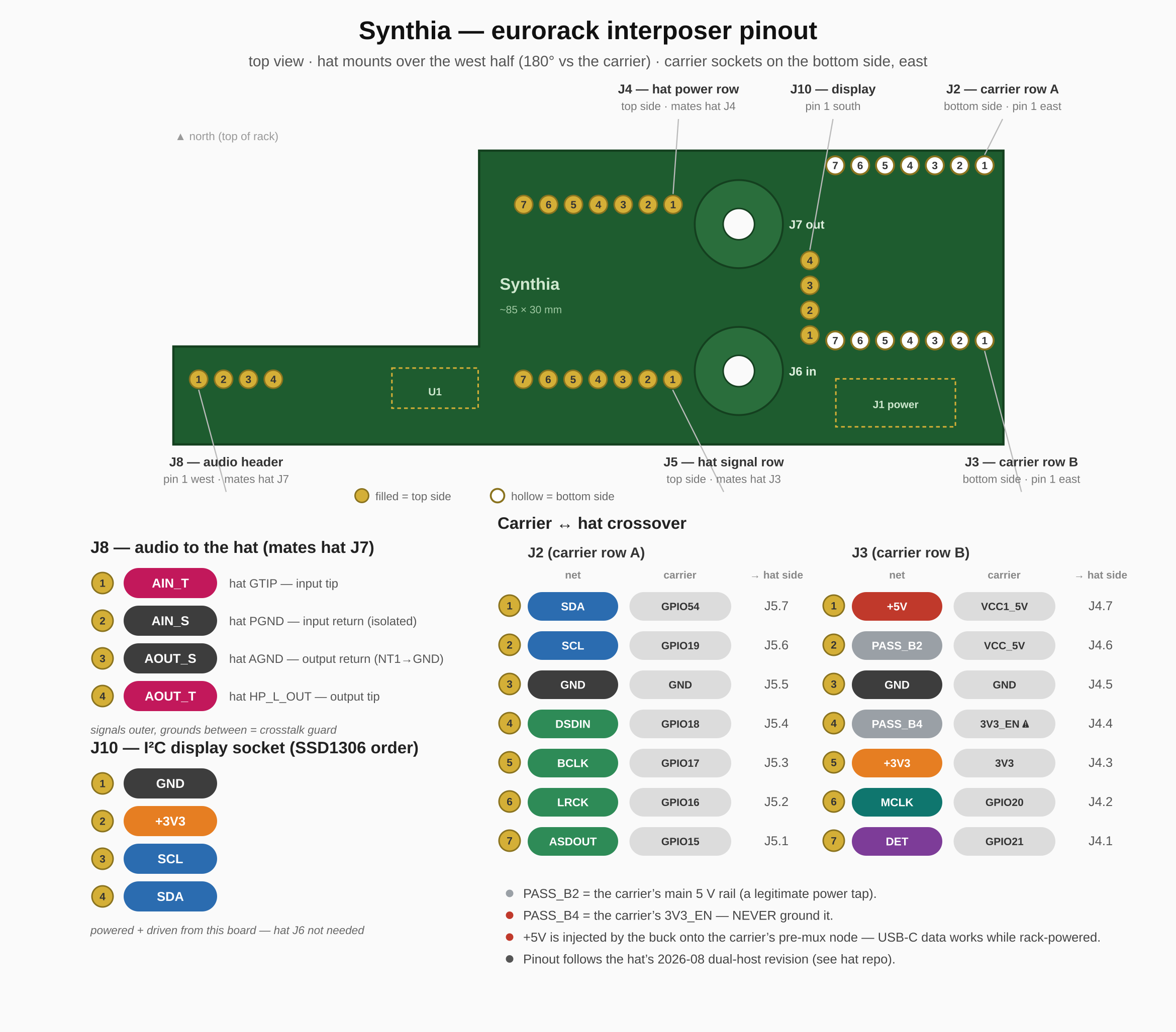
Eurorack is an open-source printed circuit board by scrambletools, from the scrambletools/AVB-Eurorack repository on GitHub. It is a 2-layer board of 84.7 × 30 mm with 29 parts on 32 nets, routed with 245 tracks and 28 vias.
It is built around the K7805-1000R3, TL072 and SS34. Its parts include 9 connectors, 7 capacitors, 6 resistors, 2 ICs and 2 diodes. It belongs with the audio and music boards of this library.
Synthia — Eurorack Interposer for the Scramble Hat-trik
A 2-layer PCB (~85 × 30 mm) that turns the ESP32-P4-ETH carrier +
Scramble Hat-trik stack into a eurorack module: rack power, panel audio
I/O, and a display socket, with no changes to either board.
text
        ┌───────────────┐
        │  Scramble Hat │   (mounted 180° opposite the carrier)
        ├─ J4/J5 male ──┤
        │   THIS BOARD  │──▶ 10-pin eurorack power in, 5 V buck out,
        ├─ J2/J3 female─┤     3.5 mm in/out jacks, I²C display socket
        │  ESP32-P4-ETH │
        └───────────────┘
Features
Eurorack power (J1, 2×5 shrouded IDC): +12 V from the bus through
reverse-polarity protection (D1) and a ferrite (FB1) into a
K7805-1000R3 buck (U1) → 5 V injected into the mezzanine, powering
the carrier and the hat. −12 V feeds the output amplifier (D2 + FB2
conditioned).
Hat interposer (J2/J3 bottom-side sockets down to the carrier;
J4/J5 headers up to the hat): a full 7+7 pass-through, cross-wired so
the hat mounts 180° opposite its normal orientation.
Panel audio (J6 in, J7 out — 3.5 mm mono threaded jacks) to header
J8, which direct-mates the hat's J7 socket. Eurorack-levelled both
ways: the input is padded −11.5 dB (R2/R3 100k/39k — ±5 V modular
swings land inside the hat's codec range) and the output is amplified
×4.9 by a TL072 on the rack's ±12 V rails (hat's ~2 Vpp → ~10 Vpp
modular level, 1 kΩ series out).
Display socket (J10): GND / 3V3 / SCL / SDA for an SSD1306-style
I²C OLED, powered and driven directly from this board — the hat's J6
header is not needed.
Usage notes
USB-C works while the module is rack-powered (bench-verified): the
buck injects on the carrier's pre-mux node (VCC1_5V, the same one the
PoE module drives), so the carrier's own power mux disconnects USB
VBUS automatically and only USB data + the UART chip stay active.
One caveat: with the rack off and USB still plugged, USB back-feeds
the buck's output — tolerated in practice but unspecified for the
K7805; unplug one or the other when parked, or add an ideal diode
(LM66100, LCSC C2869734) in the buck's output if you want it bulletproof.
Phantom power doesn't exist in the rack (no PoE), so the hat's XLR
condenser path is out of scope here — the module's jacks use the
instrument input and line output instead.
Hat build for eurorack: populate J7 + R27; leave J1 (combo
jack), SW1 and J6 unpopulated.
Levels: handled on-board. Input: R2/R3 (100k/39k, ≈ −11.5 dB) pads
±5 V modular signals into the hat's codec range. Output: U2 (TL072,
±12 V) amplifies the hat's ~2 Vpp to ~10 Vpp modular level with a 1 kΩ
series output. For non-modular sources into J6 (guitar level), swap
R2 to 0 Ω and leave R3 off — that restores the hat's native
instrument-level path.
Mezzanine crossover map
J4 sits directly above J2, J5 above J3, all pin 1s oriented the same way.
Because the hat mounts 180° opposite the carrier, the pin order reverses;
the routing un-scrambles it:
This J2 (carrier row A)
net
→ appears on
This J3 (carrier row B)
net
→ appears on
1
SDA
J5.7
1
+5V
J4.7
2
SCL
J5.6
2
PASS_B2
J4.6
3
GND
J5.5
3
GND
J4.5
4
DSDIN
J5.4
4
PASS_B4
J4.4
5
BCLK
J5.3
5
+3V3
J4.3
6
LRCK
J5.2
6
MCLK
J4.2
7
ASDOUT
J5.1
7
DET
J4.1
This follows the hat's 2026-08 mezzanine pinout revision (Pico-compatible;
see the hat README). Carrier firmware pin constants: SDA = GPIO54,
SCL = GPIO19, DSDIN = GPIO18, BCLK = GPIO17, LRCK = GPIO16,
ASDOUT = GPIO15, MCLK = GPIO20, DET = GPIO21.
PASS_B2/PASS_B4 are unused by the hat but bench-tracing identified them
on the carrier: PASS_B2 = the carrier's main 5 V rail (downstream of
its ORing diode — a legitimate power tap) and PASS_B4 = the carrier's
3V3_EN — never ground it, that would kill the carrier's 3.3 V rail.
Audio to the hat (J8)
J8 direct-mates the hat's J7 socket (same 8.5 mm stacking series as the
mezzanine, so all connectors seat together). Pin-for-pin when mated:
J8 pin
net
hat J7 pin / net
note
1
AIN_T
1 GTIP
input tip
2
AIN_S
2 PGND
input ground
3
AOUT_S
3 AGND
output ground
4
AOUT_T
4 HP_L_OUT
output tip (left channel)
Signals sit on the outer pins with both grounds between them — deliberate
crosstalk guarding; keep the order if anything gets re-pinned. Fallback:
the same pins can be hand-wired to the hat's J1/J2 pads with shielded
cable (see the hat README).
Grounding: the input side stays fully isolated (sleeve → hat PGND,
passive divider only). The output side is driven by the ±12 V amplifier,
so its return (AOUT_S / hat AGND) is bonded to module GND at one
deliberate point (net-tie NT1 beside the amp) — AIN_S and AOUT_S are
still never joined to each other. The jacks must have plastic threaded noses so the
metal faceplate doesn't short the two sleeves together — don't substitute
metal-bushing jacks.
Jacks
XKB PJ-3410 (LCSC C5146694) — a vertical PCB jack: nose points
straight up, ~19.5 mm above the PCB; plastic threaded nose M7.7 × 0.75;
faceplate hole ≥ 7.8 mm (larger than a Thonkiconn's 6 mm). Bench-verify
the pad map (T/S/TN) with a meter on a sample before ordering boards —
it was derived from the vendor footprint, not measured. Terminal 3 is
intentionally unconnected.
Power header
J1 pins 1–2 = −12 V (red-stripe end), 3–8 = GND, 9–10 = +12 V. D1
blocks a reversed ribbon from applying −12 V to the buck.
Layout notes (as built)
Carrier sockets at the east edge (the carrier extends below/east); the
hat mounts over the west half, overhanging the south edge. Constrained
placements can be re-derived against the hat file with
tools/map_hat.py.
Audio runs are tight signal+return pairs (input along the south edge,
output around the north), input and output ≥ 7 mm apart, attenuator at
the J8 end. A single B.Cu ground pour covers the power/crossover
region; the audio island is pour-free. Coupling audit passed.
Repository layout
Path
Contents
eurorack.kicad_sch / .kicad_pcb
schematic + layout
BOM.csv
bill of materials — single source of truth
fab/
JLCPCB gerbers, drills, BOM, CPL — see fab/README.md
tools/gen_fab.py
regenerate the production files
tools/map_hat.py
derive hat-constrained placements from the hat PCB
The I/O stage is placed, routed and DRC-clean. Schematic is ahead of
the PCB on one item: the hat's 2026-08 mezzanine pinout revision. The
crossover copper is untouched (the runs just carry new net names after
Update-PCB-from-Schematic), but the J10 display SCL/SDA stubs must be
re-routed — I²C moved from the J3.6/J3.7 ↔ J4.2/J4.1 runs (now
MCLK/DET) to the J2.2/J2.1 ↔ J5.6/J5.7 runs. Regenerate fab/docs
afterwards. Before ordering: bench-verify the PJ-3410 pad map, and
caliper-check the carrier's mezzanine row spacing against J2/J3
(designed 17.75 mm; the fit-proven hat uses 17.577 mm).
ESP32 controller board for a tigerexped Warmduscher Kit 2.0: 16 A relay for the 24 V/300 W boiler element plus AUTOTERM Air 4D 5 V UART control, driven from Home Assistant. KiCad PCB generated from Python.
It measures 84.7 × 30 mm and has 2 copper layers, 1.6 mm thick.
What parts does the Eurorack use?
29 parts, built around the K7805-1000R3, TL072 and SS34. The full list of its parts is on this page, with links to each part's symbol and footprint where PCBKit's library has them.
Where can I download the Eurorack KiCad files?
From the scrambletools/AVB-Eurorack repository on GitHub, at the commit this page was made from: the board is eurorack.kicad_pcb and its schematic eurorack.kicad_sch. PCBKit opens the board in the browser, with nothing to install.
Can I use the Eurorack design in my own project?
Its repository states no licence, so its author keeps all rights: ask scrambletools before reusing the design.