2 layers101.6 × 32.4 mm
 schlae/EMP-20Module15
Universal EMP-20 Family Module
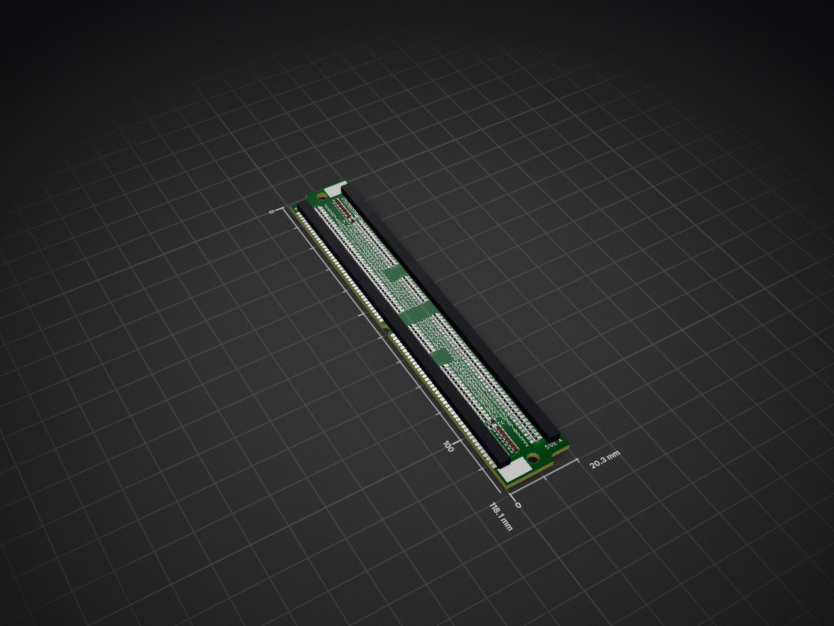
EMP-20Module is an open-source printed circuit board by schlae, from the schlae/EMP-20Module repository on GitHub. It is a 2-layer board of 20.3 × 118.1 mm with 152 parts on 152 nets, routed with 224 tracks and 4 vias.
The Needham Electronics EMP-20 is an older parallel-port connected device programmer that can be found fairly inexpensively and supports a wide range of older devices, so it is particularly useful for retrocomputing.
The EMP-20 requires a set of family modules to rewire the socket for particular types of target devices. Typically only power, ground, and VPP signals route through the family module.
Unfortunately many used EMP-20 devices are missing many family modules, making them much less useful -- until now!
I've designed a universal family module that can be wired up as many different modules by following the chart further down the page.
You can download the fabrication files here.
Please note that this board is NOT the normal 1.6mm thickness. To fit in the SIMM socket, you will need to fabricate it with a 1.2mm thickness. Some fab vendors offer this thickness and are relatively affordable -- take a look at pcbway.com for example.
Dimensions are 20.32mm x 118.11mm. Two layers, 1oz copper finish. You can go for ENIG if you wish, but the originals were HASL so that's probably fine too.
Each module has two sets of wiring, one for the A side and the other for the B side. For example, if you want to build module 01, you will need to assemble both rows 01A and 01B from the table below.
To begin wiring a module, orient the board so the text on the right side is not upside down. First thing to assemble is the ID code. Convert the ID code from the table into binary. Wherever there is a logical '1', solder across the appropriate IDx jumpers on the top right of the board. For example, if you're assembling module 09A, you have module ID 17, which is 10001 in binary. This means that you will solder jumpers on ID0 and ID4.
Next, go through the list of grounds and solder a short across that pin. For example, if the number '2' is in the list of grounds, solder a jumper wire or place a 0 ohm resistor across the two pads labeled '2' on the board.
For the point-to-point wiring, solder a wire from the right-most pad next to the number called out, then run it to the right-most pad next to the other number that is called out. For example, 17->72 means you have to solder a jumper wire from the right-most pad next to the number 17 and run it to the right-most pad next to the number 72.
Some modules have passive components on them. 14->150pF->GND means that you need to solder a 150pF surface mount capacitor across the pads next to the number 14. 12->100 ohm->70 means that you need to solder a 100 ohm resistor to the right-most pad next to number 12, then solder a jumper wire to the other terminal of the resistor (DO NOT let it touch the left pad) and run it to the right-most pad next to number 70. It's basically just a jumper wire with a resistor in series.

In the picture, the family module is partially assembled. Only the A side has any wiring, and it is set to ID 5. A 150pF capacitor to ground is installed at pad 14, and a jumper wire goes from pad 16 to pad 72.
When you've finished that side, you may want to check it with a multimeter to make sure you didn't make any mistakes. Then rotate the board 180 degrees and repeat the process with side B.
You'll want to test the module first with a device that you don't care about just in case something's not wired correctly. If you can program and verify successfully, then congratulations!
| Module ID | Name | ID code | Grounds | Point-to-point | Special |
|---|---|---|---|---|---|
| 01A | Standard EPROM | 1 | 2 | 17->72, 19->62, 25->70, 28->58, 29->68, 32->56, 33->66 | |
| 01B | 16 bit EPROMS | 2 | 21, 21 | 3->68, 23->62, 40->58, 45->70 | |
| 02A | Intel 8048/49/51/52 uP | 3 | 2, 19 | 11->72, 13->70, 23->68, 28->62, 32->58, 45->54 | |
| 02B | 87X7xx | 4 | 66 | 2->70, 6->68, 14->72, 18->58, 25->56, 29->54 | |
| 03A | PAL 16V8/20V8/22V10 | 5 | 2 | 6->62, 16->72, 18->68, 20->58, 21->56, 22->70, 25->54, | 14->150pF->GND |
| 03B | GAL 16V8/22V10, etc | 6 | 2 | 3->62, 5->55, 7->61, 18->72, 21->70, 22->58, 24->56, 25->68, 28->64, 29->66 | |
| 04A | PIC16C5x family | 7 | 45, 64 | 10->72, 11->62, 22->58, 26->56, 33->66 | 12->100 ohm->70, 29->100 ohm->68 |
| 04B | Serial EEPROMS | 8 | 16, 19, 66 | 2->70, 3->68, 5->56, 7->72, 9->62, 17->18->54, 21->58 | |
| 05A | Zilog Z86 | ||||
| 05B | Zilog Z86 | ||||
| 06A | Zilog Z86 | ||||
| 06B | Zilog Z86 | ||||
| 07A | Xicor PAL | ||||
| 07B | n/a | ||||
| 08A | Cypress EPROMS | ||||
| 08B | Large EPROM/flash | ||||
| 09A | 68HC705, MACH | 17 | 2, 46 | 4->72, 19->70, 26->58, 29->62, 36->68, 38->60, 45->56 | |
| 09B | 67HC711 | 18 | 41, 64 | 3->44->56, 10->70, 11->62, 13->72, 22->68, 40->58 | |
| 10A | EEPROM | ||||
| 10B | n/a | ||||
| 11A | PEEL devices | 21 | 2 | 3->68, 4->70, 14->72, 18->58, 20->62, 21->56, 24->60, 25->54 | |
| 11B | TMS7782 | 22 | 45, 64 | 2->72, 11->68, 15->58, 16->70, 18->62, 28->56, 33->54 | |
| 12A | PSD | ||||
| 12B | n/a | ||||
| 13A | Altera EP devices | ||||
| 13B | Altera | ||||
| 14A | Atmel 22V10 | 27 | 2 | 4->72, 14->70, 16->58, 24->56, 25->60 | 3-> -|<- 1N5818 ->68 |
| 14B | ATV2500 | 28 | 21 | 3->56, 5->58, 22->60, 36->72, 37->70 | 2-> -|<- 1N5818 ->68 |
| 15A | 29F100/200 | ||||
| 15B | EP1800 | ||||
| 16A | GAL26V12 | 31 | 15 | 16->68, 26->58 | |
| 16B | PIC16C6x/PIC17Cxx | 32 | 22, 23 | 25->54, 40->68 | |
| 17A | 62Txx | ||||
| 17B | 62T/Exx | ||||
| 18A | PEEL/ATTiny/X76 | 35 | 2 | 5->68, 6->70, 8->62, 9->56, 16->72, 24->60, 25->54 | |
| 18B | PIC16Cxx | 36 | 66 | 13->58, 14->68, 18->23->70, 20->25->72, 28->56, 40->54 | |
| 19A | XC72xx | ||||
| 19B | XC95xx (Xilinx) | ||||
| 20A | XC72xx | ||||
| 20B | n/a | ||||
| 21A | n/a | ||||
| 21B | AT17Cxx | ||||
| 22A | 29F002 | ||||
| 22B | 29F1xx | ||||
| 23A | Atmel 150x family | ||||
| 23B | ATV2500 | ||||
| 24A | COP87xx | ||||
| 24B | COP87xx | ||||
| 25A | AT22V10B | ||||
| 25B | P51-XA-G1 | ||||
| 26A | PIC14000 | ||||
| 26B | 22V10 | ||||
| 27A | 26C512 | ||||
| 27B | Z86 | ||||
| 28A | PIC12C families | 55 | 20, 21, 64 | 2->56, 3->68, 8->70, 9->72, 46->62 | |
| 28B | P28F002 | 56 | 6, 32 | 18->20->68, 23->62, 25->58 | |
| 29A | 29F070-psop44 | ||||
| 29B | 27SF010 |
This chart is incomplete. I have ohmed out all the modules I have, but I am counting on the community to provide the rest. If you have a module that's not on the list, ohm out the connections! You can submit a pull request or contact me directly.
This work is licensed under a Creative Commons Attribution 4.0 International License. See https://creativecommons.org/licenses/by/4.0/.
| Qty | Value | Footprint | References |
|---|---|---|---|
| 2 | 10 | Passive:RESC1608X55_HandSoldering | JP66, JP140 |
| 2 | 11 | Passive:RESC1608X55_HandSoldering | JP65, JP139 |
| 2 | 12 | Passive:RESC1608X55_HandSoldering | JP64, JP138 |
| 2 | 13 | Passive:RESC1608X55_HandSoldering | JP63, JP137 |
| 2 | 14 | Passive:RESC1608X55_HandSoldering | JP62, JP136 |
| 2 | 15 | Passive:RESC1608X55_HandSoldering | JP61, JP135 |
| 2 | 16 | Passive:RESC1608X55_HandSoldering | JP60, JP134 |
| 2 | 17 | Passive:RESC1608X55_HandSoldering | JP59, JP133 |
| 2 | 18 | Passive:RESC1608X55_HandSoldering | JP58, JP132 |
| 2 | 19 | Passive:RESC1608X55_HandSoldering | JP57, JP131 |
| 2 | 2 | Passive:RESC1608X55_HandSoldering | JP74, JP148 |
| 2 | 20 | Passive:RESC1608X55_HandSoldering | JP56, JP130 |
| 2 | 21 | Passive:RESC1608X55_HandSoldering | JP55, JP129 |
| 2 | 22 | Passive:RESC1608X55_HandSoldering | JP54, JP128 |
| 2 | 23 | Passive:RESC1608X55_HandSoldering | JP53, JP127 |
| 2 | 24 | Passive:RESC1608X55_HandSoldering | JP52, JP126 |
| 2 | 25 | Passive:RESC1608X55_HandSoldering | JP51, JP125 |
| 2 | 26 | Passive:RESC1608X55_HandSoldering | JP50, JP124 |
| 2 | 27 | Passive:RESC1608X55_HandSoldering | JP49, JP123 |
| 2 | 28 | Passive:RESC1608X55_HandSoldering | JP48, JP122 |
| 2 | 29 | Passive:RESC1608X55_HandSoldering | JP47, JP121 |
| 2 | 3 | Passive:RESC1608X55_HandSoldering | JP73, JP147 |
| 2 | 30 | Passive:RESC1608X55_HandSoldering | JP46, JP120 |
| 2 | 31 | Passive:RESC1608X55_HandSoldering | JP45, JP119 |
| 2 | 32 | Passive:RESC1608X55_HandSoldering | JP44, JP118 |
| 2 | 33 | Passive:RESC1608X55_HandSoldering | JP43, JP117 |
| 2 | 34 | Passive:RESC1608X55_HandSoldering | JP42, JP116 |
| 2 | 35 | Passive:RESC1608X55_HandSoldering | JP41, JP115 |
| 2 | 36 | Passive:RESC1608X55_HandSoldering | JP40, JP114 |
| 2 | 37 | Passive:RESC1608X55_HandSoldering | JP39, JP113 |
| 2 | 38 | Passive:RESC1608X55_HandSoldering | JP38, JP112 |
| 2 | 39 | Passive:RESC1608X55_HandSoldering | JP37, JP111 |
| 2 | 4 | Passive:RESC1608X55_HandSoldering | JP72, JP146 |
| 2 | 40 | Passive:RESC1608X55_HandSoldering | JP36, JP110 |
| 2 | 41 | Passive:RESC1608X55_HandSoldering | JP35, JP109 |
| 2 | 42 | Passive:RESC1608X55_HandSoldering | JP34, JP108 |
| 2 | 43 | Passive:RESC1608X55_HandSoldering | JP33, JP107 |
| 2 | 44 | Passive:RESC1608X55_HandSoldering | JP32, JP106 |
| 2 | 45 | Passive:RESC1608X55_HandSoldering | JP31, JP105 |
| 2 | 46 | Passive:RESC1608X55_HandSoldering | JP30, JP104 |
| 2 | 47 | Passive:RESC1608X55_HandSoldering | JP29, JP103 |
| 2 | 48 | Passive:RESC1608X55_HandSoldering | JP28, JP102 |
| 2 | 49 | Passive:RESC1608X55_HandSoldering | JP27, JP101 |
| 2 | 5 | Passive:RESC1608X55_HandSoldering | JP71, JP145 |
| 2 | 54 | Passive:RESC1608X55_HandSoldering | JP26, JP100 |
| 2 | 55 | Passive:RESC1608X55_HandSoldering | JP25, JP99 |
| 2 | 56 | Passive:RESC1608X55_HandSoldering | JP24, JP98 |
| 2 | 57 | Passive:RESC1608X55_HandSoldering | JP23, JP97 |
| 2 | 58 | Passive:RESC1608X55_HandSoldering | JP22, JP96 |
| 2 | 59 | Passive:RESC1608X55_HandSoldering | JP21, JP95 |
| 2 | 6 | Passive:RESC1608X55_HandSoldering | JP70, JP144 |
| 2 | 60 | Passive:RESC1608X55_HandSoldering | JP20, JP94 |
| 2 | 61 | Passive:RESC1608X55_HandSoldering | JP19, JP93 |
| 2 | 62 | Passive:RESC1608X55_HandSoldering | JP18, JP92 |
| 2 | 63 | Passive:RESC1608X55_HandSoldering | JP17, JP91 |
| 2 | 64 | Passive:RESC1608X55_HandSoldering | JP16, JP90 |
| 2 | 65 | Passive:RESC1608X55_HandSoldering | JP15, JP89 |
| 2 | 66 | Passive:RESC1608X55_HandSoldering | JP14, JP88 |
| 2 | 67 | Passive:RESC1608X55_HandSoldering | JP13, JP87 |
| 2 | 68 | Passive:RESC1608X55_HandSoldering | JP12, JP86 |
| 2 | 69 | Passive:RESC1608X55_HandSoldering | JP11, JP85 |
| 2 | 7 | Passive:RESC1608X55_HandSoldering | JP69, JP143 |
| 2 | 70 | Passive:RESC1608X55_HandSoldering | JP10, JP84 |
| 2 | 72 | Passive:RESC1608X55_HandSoldering | JP8, JP82 |
| 2 | 8 | Passive:RESC1608X55_HandSoldering | JP68, JP142 |
| 2 | 9 | Passive:RESC1608X55_HandSoldering | JP67, JP141 |
| 2 | ID0 | Conn:JMP1608 | JP1, JP75 |
| 2 | ID1 | Conn:JMP1608 | JP2, JP76 |
| 2 | ID2 | Conn:JMP1608 | JP3, JP77 |
| 2 | ID3 | Conn:JMP1608 | JP4, JP78 |
| 2 | ID4 | Conn:JMP1608 | JP5, JP79 |
| 2 | ID5 | Conn:JMP1608 | JP6, JP80 |
| 2 | ID6 | Conn:JMP1608 | JP7, JP81 |
| 2 | ID7 | Conn:JMP1608 | JP9, JP83 |
| 2 | MountingHole | Conn:MH_125 | H1, H2 |
| 1 | SIDE A | Conn:EDGE_DIMM_80_127 | J1 |
| 1 | SIDE B | Conn:EDGE_DIMM_80_127 | J2 |
It measures 20.3 × 118.1 mm and has 2 copper layers, 1.6 mm thick.
152 parts. The full list of its parts is on this page, with links to each part's symbol and footprint where PCBKit's library has them.
From the schlae/EMP-20Module repository on GitHub, at the commit this page was made from: the board is EMP-20 Module.kicad_pcb. PCBKit opens the board in the browser, with nothing to install.
Its repository states no licence, so its author keeps all rights: ask schlae before reusing the design.


TweetyDaBird/Lotus-58-Classic
A split ergo linear keyboard derived from the Lily58 family


ktec-hq/ErgoDone
ErgoDox using pro micro. Original work by Dox. Brainhole association present


