
2 layers97 × 52.5 mm
 sandhya-na/PCB-projects
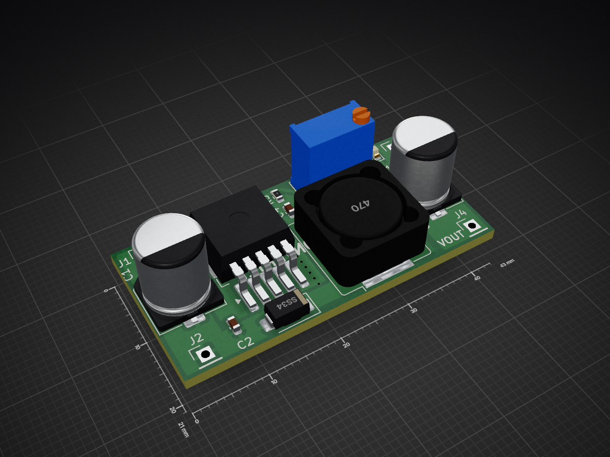
Buck converter pcblayout is an open-source printed circuit board by sandhya-na, from the sandhya-na/PCB-projects repository on GitHub. It is a 2-layer board of 43 × 21 mm with 15 parts on 6 nets, routed with 18 tracks and 9 vias.
It is built around the SS34. Its parts include 4 capacitors, 4 connectors, 2 resistors, 2 diodes and 1 IC. It belongs with the power boards of this library.
This repository contains my original hardware designs developed in KiCad 10. These projects focus on power regulation and PCB layout best practices, including thermal management and signal integrity.
This project is a regulated power supply designed to convert 12V AC input into a stable 5V DC output.
  * Rectification Stage:
        Uses a full-bridge rectifier consisting of four 1N4007 diodes to convert the AC input to pulsating DC.
  * Regulation:
        Features an LM7805 linear regulator in a TO-220 package to provide a constant 5V output.
  * Filtering System:
     - A large 1000µF electrolytic capacitor (C1) is used for bulk smoothing of the rectified AC ripple.
     -  0.1µF ceramic capacitors (C2, C3) are placed close to the regulator pins to filter out high-frequency noise.
  * Circuit Protection:
        Includes an input fuse (F1) to protect the components from overcurrent or short-circuit conditions.
  * Visual Indication:
An on-board LED with a 2.2kΩ resistor provides immediate status of the output power.The layout focuses on safety and stability. I prioritized proper spacing between the AC input terminals and the DC output to prevent interference and ensured the LM7805 has enough space for heat dissipation.
This project is a high-efficiency switching regulator based on the LM2596-ADJ IC, used for stepping down DC voltages.
*  Switching Regulator:
       Powered by the LM2596S-ADJ, which operates at a switching frequency of 150kHz for high efficiency.
* Adjustable Output:
      Uses a 10kΩ potentiometer (RV1) in the feedback loop, allowing the user to precisely set the desired output voltage.
* Power Components :
   - A 47µH inductor (L1) and a Schottky diode (D2) are used for energy storage and current steering during the switching cycle.         -  Features a 100µF input cap and a 220µF output cap to stabilize the switching waveforms.
* Indication:
Includes a power-on LED with a 4.7kΩ resistor.For this layout, I focused on Power Integrity:
Contact: sandhyana384@gmail.com
| Qty | Value | Footprint | References |
|---|---|---|---|
| 2 | Connector_PinHeader_2.54mm:PinHeader_1x01_P2.54mm_Vertical | J3, J4 | |
| 2 | 100nF | Capacitor_SMD:C_0603_1608Metric | C2, C4 |
| 1 | Package_TO_SOT_SMD:TO-263-5_TabPin3 | U1 | |
| 1 | Connector_PinHeader_2.54mm:PinHeader_1x01_P2.54mm_Vertical | J1 | |
| 1 | Connector_PinHeader_2.54mm:PinHeader_1x01_P2.54mm_Vertical | J2 | |
| 1 | 100uF | Capacitor_SMD:CP_Elec_8x10 | C1 |
| 1 | 10K | Potentiometer_THT:Potentiometer_Bourns_3296W_Vertical | RV1 |
| 1 | 1K | Resistor_SMD:R_0603_1608Metric | R3 |
| 1 | 220uF | Capacitor_SMD:CP_Elec_8x10 | C3 |
| 1 | 47uH | Inductor_SMD:L_Bourns_SRR1208_12.7x12.7mm | L1 |
| 1 | 4K7 | Resistor_SMD:R_0603_1608Metric | R1 |
| 1 | LED | LED_SMD:LED_0603_1608Metric | D1 |
| 1 | SS34 | Diode_SMD:D_SMA | D2 |

willem-pennings/balancing-cube
A cube that balances itself in a corner or edge using reaction wheels

Arrow-air/project-quiver
Project Quiver documentation, designs, and project artifacts.


Arrow-air/project-caribou
Project Caribou documentation, designs, and project artifacts.

FujiNetWIFI/fujinet-hardware
Schematics and design files for FujiNet hardware


CrashOverride85/zc95
4 channel EStim box inspired by the mk312bt, with Lua scripting support

It measures 43 × 21 mm and has 2 copper layers, 1.6 mm thick.
15 parts, built around the SS34. The full list of its parts is on this page, with links to each part's symbol and footprint where PCBKit's library has them.
From the sandhya-na/PCB-projects repository on GitHub, at the commit this page was made from: the board is Buck_Converter/buck_converter_pcblayout.kicad_pcb and its schematic ACtoDC_converter/ACtoDC_schematic.kicad_sch. PCBKit opens the board in the browser, with nothing to install.
Its repository states no licence, so its author keeps all rights: ask sandhya-na before reusing the design.