2 layers42 × 47 mm

 sanbungi/myslimetracker
Mydcdc is an open-source printed circuit board by sanbungi, from the sanbungi/myslimetracker repository on GitHub. It is a 2-layer board of 20 × 15 mm with 12 parts on 6 nets, routed with 40 tracks and 7 vias.
Its parts include 5 connectors, 3 capacitors, 1 IC and 1 inductor.
VR ヘッドセットだけでは追跡できない足や腰の動きを取るための、自作 SlimeVR 互換フルボディトラッカーです。両足先・両膝・腰・胸の6点に装着し、VRChat 上でのフルトラッキングを実現しています。
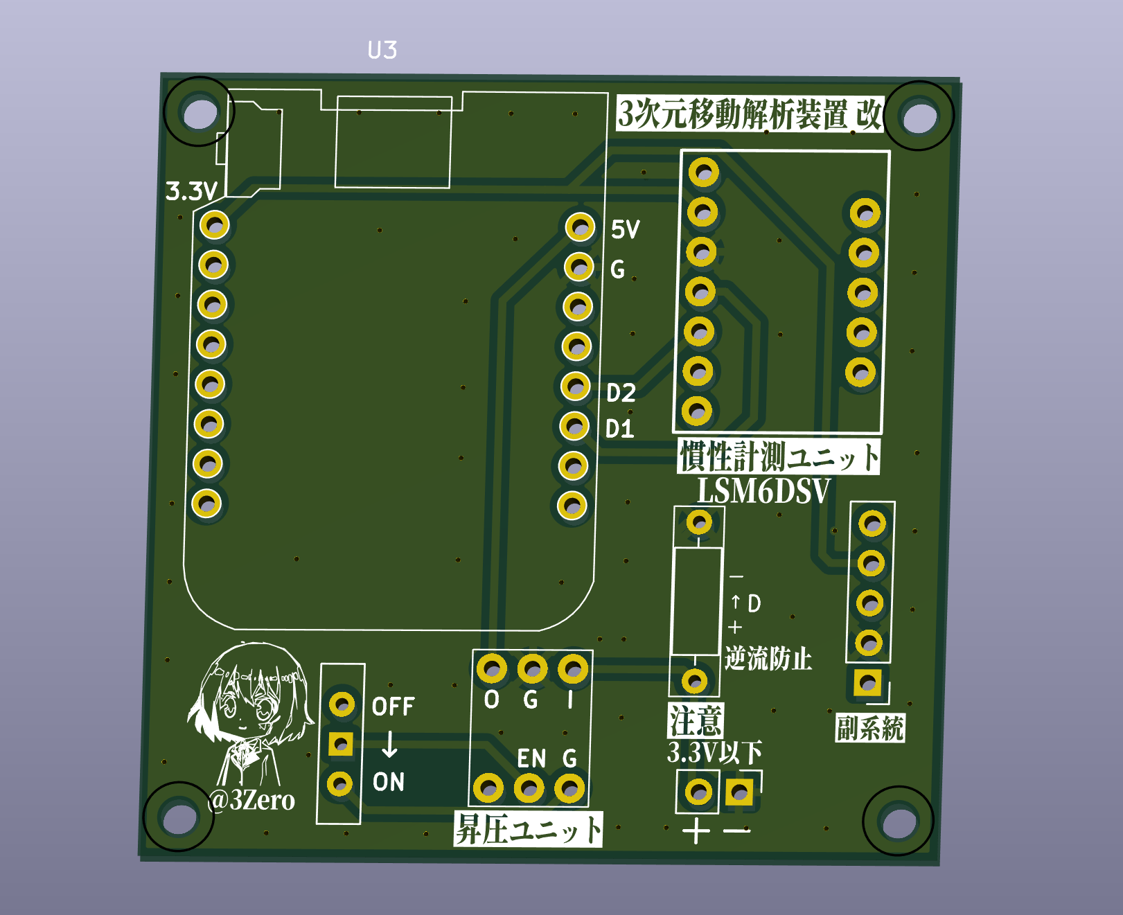
現行基板の3Dレンダリング(KiCad)
https://github.com/user-attachments/assets/3b7e9f30-eae3-4ba1-b326-60af60dc9e0d
VRChat 内でのフルボディトラッキング動作
SlimeVR トラッカーの自作例はほとんどがリチウムポリマー電池を電源としていますが、本プロジェクトでは 単3乾電池 を採用しています。発火・膨張のリスクがなく、どこでも手に入り、近年は充電式乾電池(eneloop 等)も安価に出回っているため、ランニングコストも実用的です。
現行版は単3電池2本で動作し、昇圧 DC-DC コンバータで MCU・IMU に必要な電圧を供給しています。
回路設計と基板レイアウトは KiCad で行い、製造は JLCPCB に発注しています。
| 部品 | 型番 | 役割 |
|---|---|---|
| MCU | Xiao ESP32-C3 | Wi-Fi 通信・SlimeVR ファームウェアの実行 |
| IMU | LSM6DSV | 6軸慣性計測(加速度 + ジャイロ) |
| 昇圧 DC-DC(現行) | 秋月電子 XCL103 キット | 単3x2 の電圧を 5V に昇圧 |
| 昇圧 DC-DC(次期) | TPS61291 | 単3x1 の電圧を 3.3V に昇圧 |
単3乾電池1本 で駆動する次期基板を開発中です。昇圧回路・MCU・IMU を1枚の基板に統合し、さらなる小型化と軽量化を目指しています。就職活動のため一時中断中ですが、設計データは new_prototype/ に格納しています。
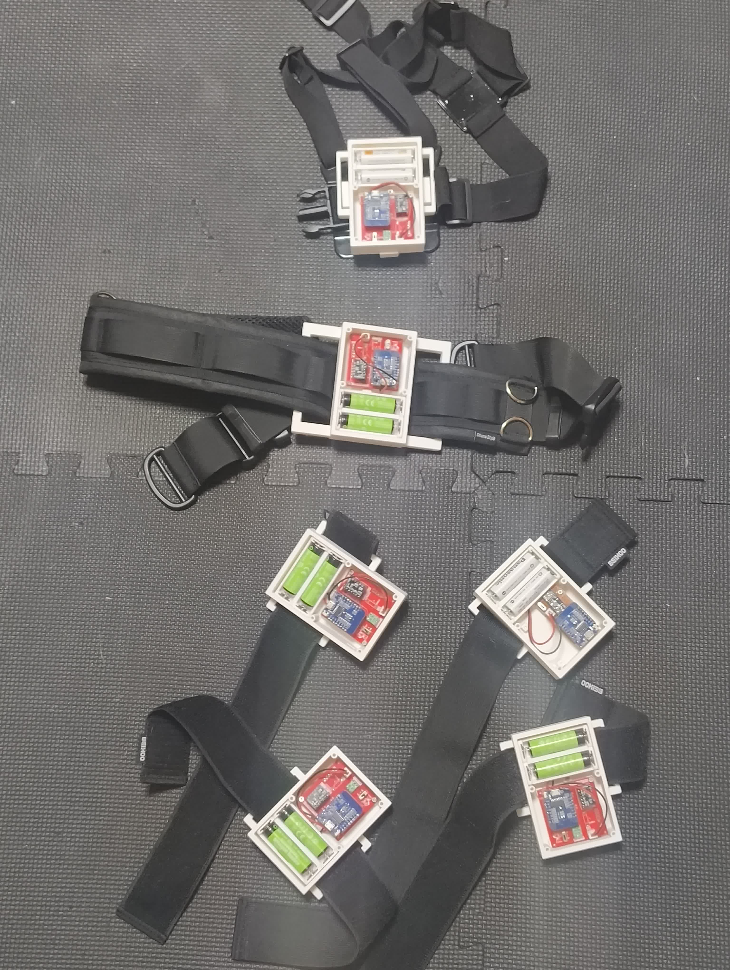
実際に運用中の6点セット(両足先・両膝・腰・胸)
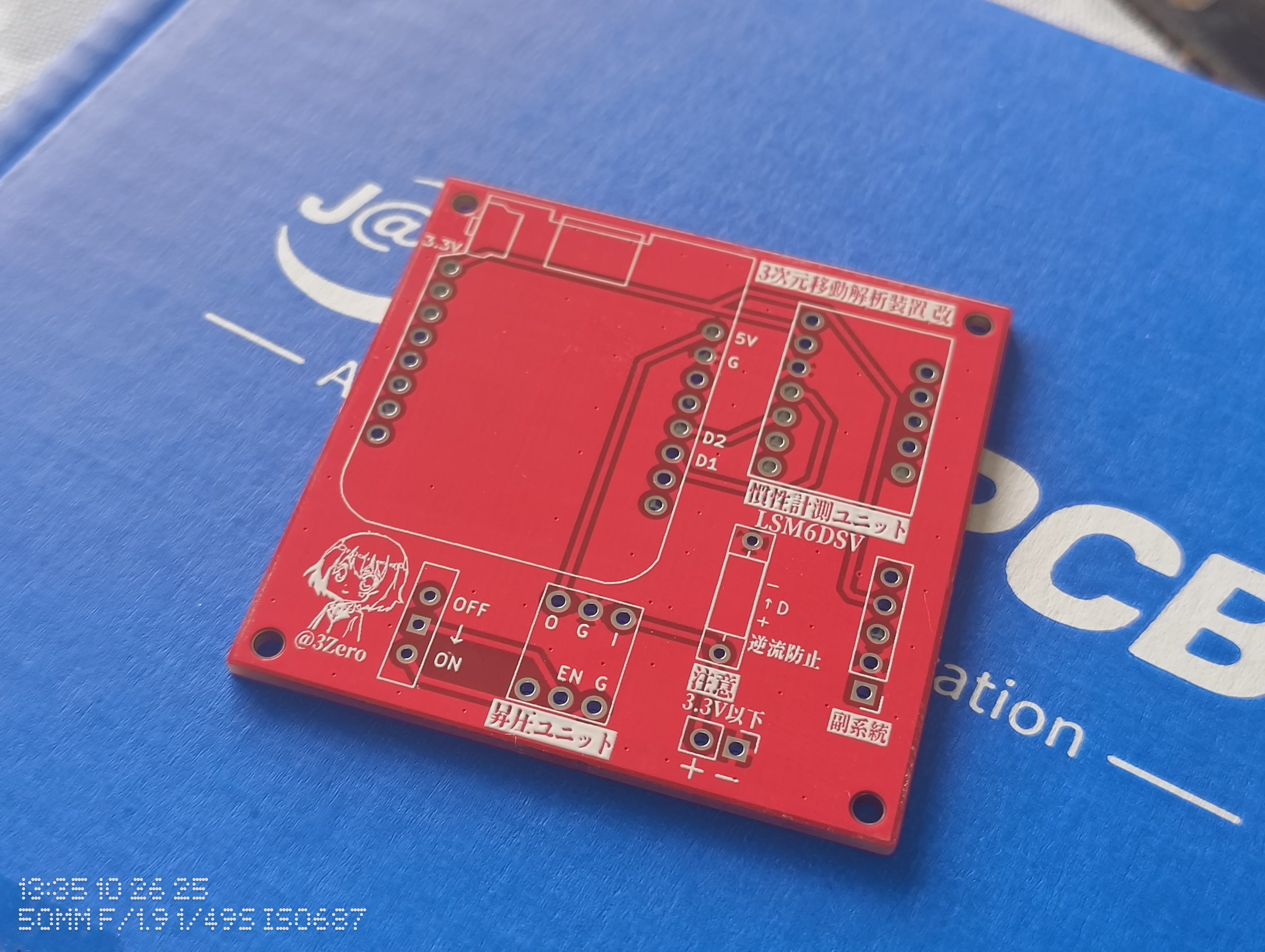
JLCPCB に発注した基板の実物。
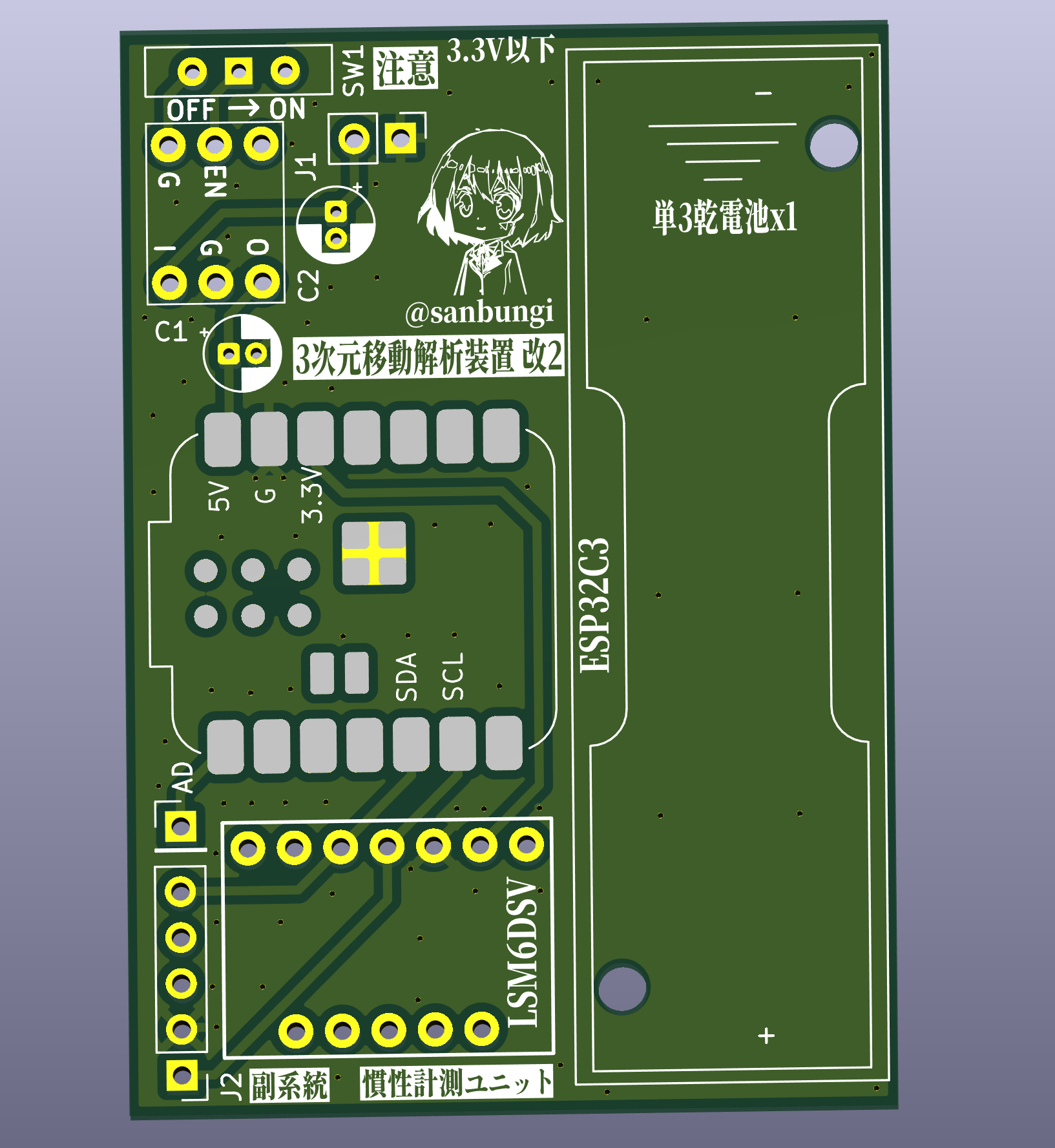
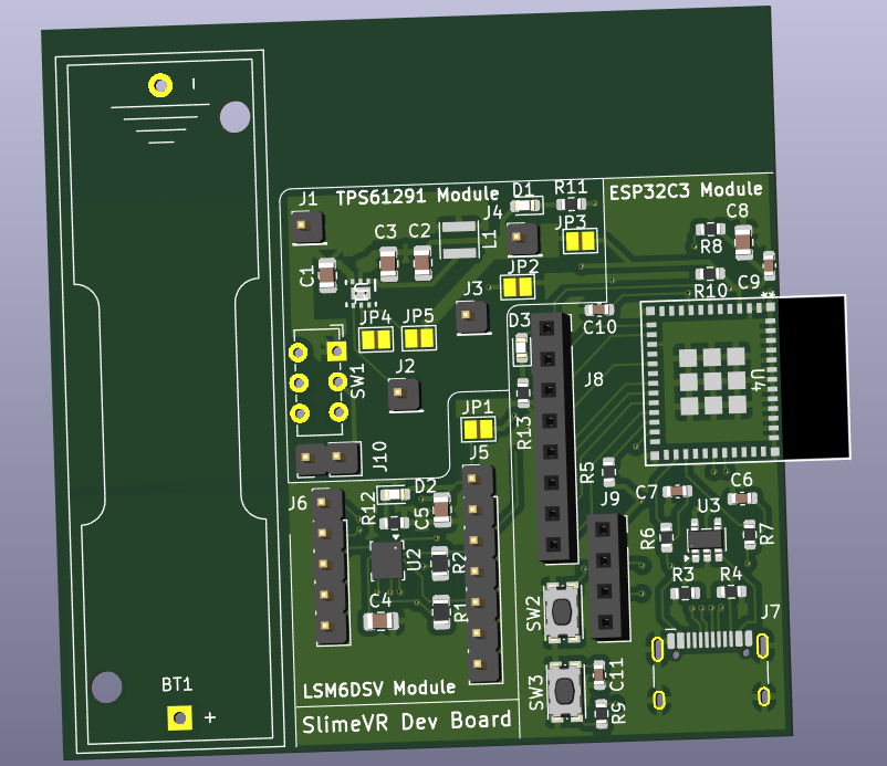
左: 単3乾電池1本用の次期統合基板 / 右: 部品実装後のイメージ
KiCad 上での3Dレンダリング。昇圧ユニット・IMU・逆流防止回路を搭載。
| Qty | Value | Footprint | References |
|---|---|---|---|
| 5 | Conn_01x01 | Connector_PinHeader_2.54mm:PinHeader_1x01_P2.54mm_Vertical | J1, J2, J3, J4, J5 |
| 2 | 22uF | Capacitor_SMD:C_0805_2012Metric | C2, C3 |
| 2 | Jumper_2_Open | Jumper:SolderJumper-2_P1.3mm_Open_Pad1.0x1.5mm | JP1, JP2 |
| 1 | 10uF | Capacitor_SMD:C_0805_2012Metric | C1 |
| 1 | 3.3uH | Inductor_SMD:L_Taiyo-Yuden_MD-3030 | L1 |
| 1 | TPS61291DRVR | footprints:DRV0006A | U1 |


github-linguist/linguist
Language Savant. If your repository's language is being reported incorrectly, send us a pull request!


google/mozc-devices
Circuit diagrams and firmware source code for Gboard DIY keyboards


hackclub/OnBoard
💡 Join 1,000 teenagers and make your first PCB with a $100 grant!

VoronDesign/Voron-Tap
Tap is a nozzle-based z-probe for the V2 and Trident printer designs. The entire toolhead moves to trigger an optical switch. Tap offers many advantages:

stacksmashing/pico-tpmsniffer
A simple, very experimental TPM sniffer for LPC bus
It measures 20 × 15 mm and has 2 copper layers, 1.6 mm thick.
12 parts. The full list of its parts is on this page, with links to each part's symbol and footprint where PCBKit's library has them.
From the sanbungi/myslimetracker repository on GitHub, at the commit this page was made from: the board is new_prototype/mydcdc/mydcdc.kicad_pcb and its schematic my_trakcer/v4/my_trakcer.kicad_sch. PCBKit opens the board in the browser, with nothing to install.
Its repository states no licence, so its author keeps all rights: ask sanbungi before reusing the design.