2 layers57 × 55.2 mm
LogicAnalyzer
gusmanb/logicanalyzer
24 channel, 100Msps logic analyzer hardware and software
10 parts5.1kGPL-3.0

 sahilkandale/Learning-log
The design process was carried out in two main stages: Schematic Design: Components were selected and electrically connected in KiCad according to the required circuit.
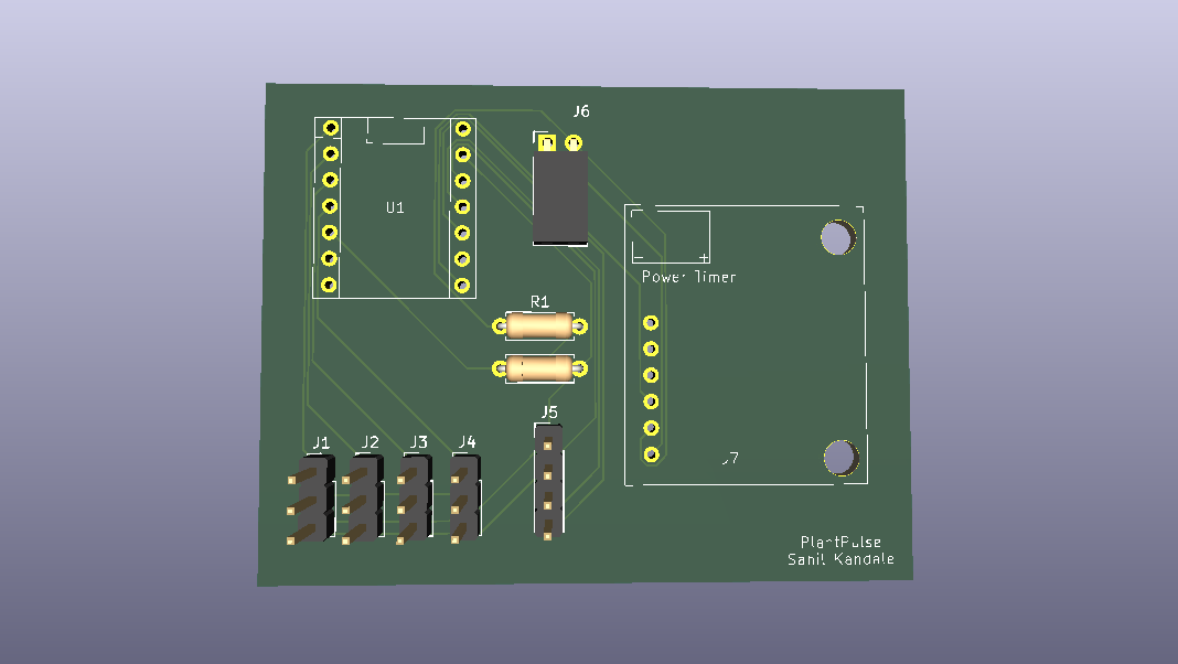
Task1 pcb is an open-source printed circuit board by sahilkandale, from the sahilkandale/Learning-log repository on GitHub. It is a 2-layer board of 62.5 × 48 mm with 10 parts on 19 nets, routed with 84 tracks and 0 vias.
Its parts include 7 connectors, 2 resistors and 1 IC.
Plant Pulse is a plant monitoring system designed to monitor the condition of a plant using electronic sensors.The circuit was designed and simulated using KiCad.
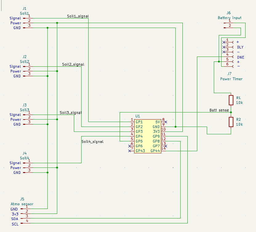
The Plant Pulse system uses sensors to detect the required plant-related conditions.
The design process was carried out in two main stages: Schematic Design: Components were selected and electrically connected in KiCad according to the required circuit. PCB Design: The schematic was converted into a PCB layout. Components were arranged properly and the connections were routed to create the final PCB design.
KiCad's design checking tools were used during the design process to identify connection and layout issues.
Learning
Challenges
| Qty | Value | Footprint | References |
|---|---|---|---|
| 2 | 10k | Resistor_THT:R_Axial_DIN0207_L6.3mm_D2.5mm_P7.62mm_Horizontal | R1, R2 |
| 1 | Atmo sensor | Connector_PinHeader_2.54mm:PinHeader_1x04_P2.54mm_Vertical | J5 |
| 1 | Battery input | Connector_PinSocket_2.54mm:PinSocket_1x02_P2.54mm_Horizontal | J6 |
| 1 | Power Timer | footprint:power timer | J7 |
| 1 | Soil1 | Connector_PinHeader_2.54mm:PinHeader_1x03_P2.54mm_Vertical | J1 |
| 1 | Soil2 | Connector_PinHeader_2.54mm:PinHeader_1x03_P2.54mm_Vertical | J2 |
| 1 | Soil3 | Connector_PinHeader_2.54mm:PinHeader_1x03_P2.54mm_Vertical | J3 |
| 1 | Soil4 | Connector_PinHeader_2.54mm:PinHeader_1x03_P2.54mm_Vertical | J4 |
| 1 | ~ | footprint:ESP32 XIAO | U1 |
It measures 62.5 × 48 mm and has 2 copper layers, 1.6 mm thick.
10 parts. The full list of its parts is on this page, with links to each part's symbol and footprint where PCBKit's library has them.
From the sahilkandale/Learning-log repository on GitHub, at the commit this page was made from: the board is task1_pcb.kicad_pcb and its schematic task1.kicad_sch. PCBKit opens the board in the browser, with nothing to install.
Its repository states no licence, so its author keeps all rights: ask sahilkandale before reusing the design.
gusmanb/logicanalyzer
24 channel, 100Msps logic analyzer hardware and software

byrantech/laptop
anyon_e, a highly integrated, high end, open source laptop. Attempt the impossible.

joeycastillo/Sensor-Watch
A board replacement for the classic Casio F-91W wristwatch


OLIMEX/OLINUXINO
OLINUXINO is Open Source / Open Hardware, low cost from EUR 24 Linux Industrial grade Single Board Computer capable to operate -25+85C

rusefi/rusefi
rusefi - GPL internal combustion engine control unit

VoronDesign/Voron-Hardware
Cool Hardware designed by the Voron Design group

hoglet67/RGBtoHDMI
Bare-metal Raspberry Pi project that provides pixel-perfect sampling of Retro Computer RGB/YUV video and conversion to HDMI