
2 layers57 × 55.2 mm
LogicAnalyzer
gusmanb/logicanalyzer
24 channel, 100Msps logic analyzer hardware and software
10 parts5.1kGPL-3.0

 yaqwsx/KiKit2.1k
Automation tools for KiCAD
Conn is an open-source printed circuit board by yaqwsx, from the yaqwsx/KiKit repository on GitHub, published under the MIT licence. It is a 2-layer board of 26 × 18 mm with 10 parts on 10 nets, routed with 147 tracks and 9 vias.

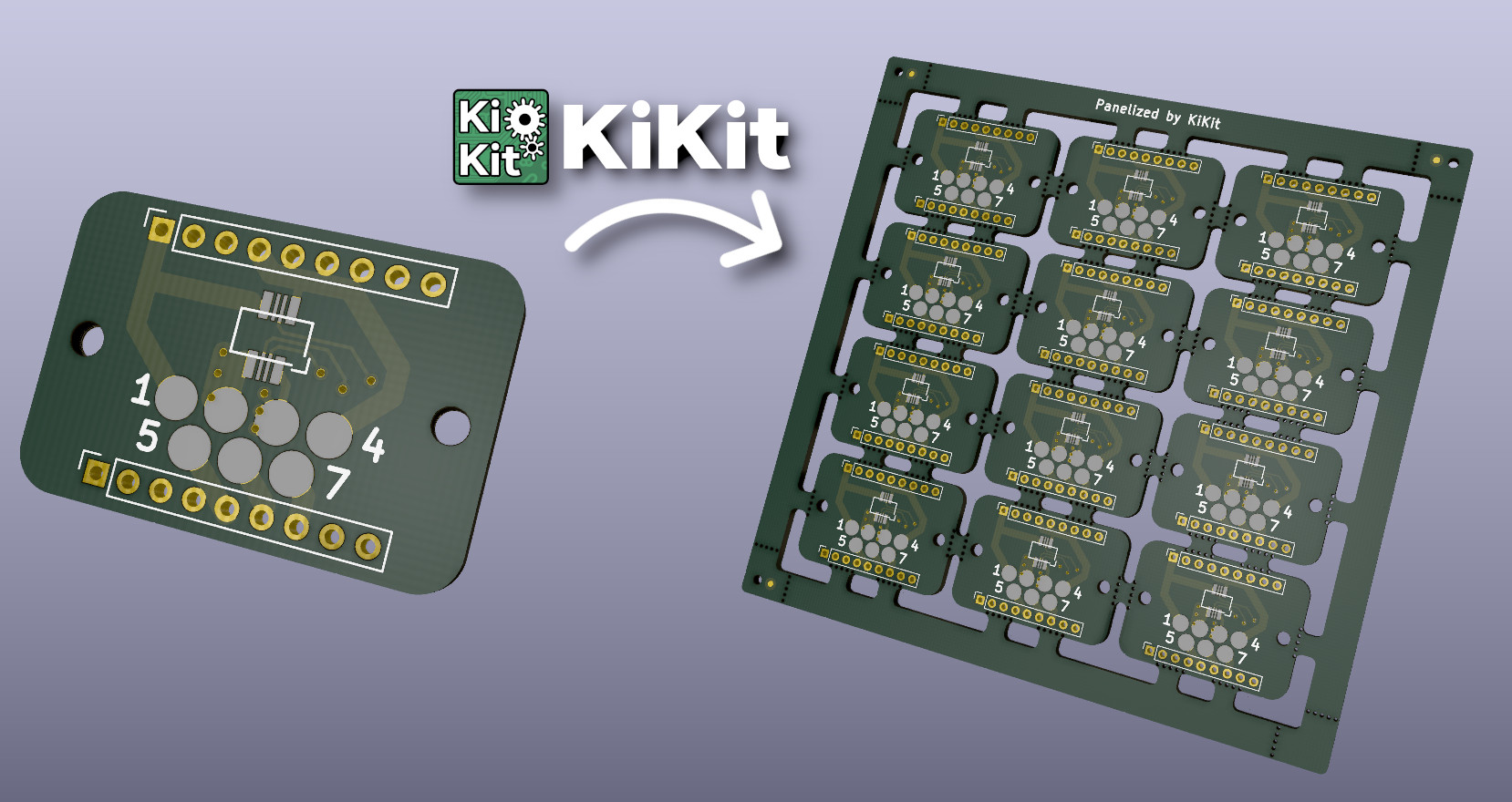
KiKit is a Python library, KiCAD plugin and a CLI tool to automate several tasks in a standard KiCAD workflow like:
Then definitely consider:

Your support will allow me to allocate time to properly maintain my projects like this.
PS: Be sure to check out my other KiCAD & PCB related projects:
KiKit is available as a PyPi package. However, due to packaging of KiCAD, installation on some platforms requires usage of specific Python interpreter.
Please follow the detailed installation guide that covers installation based on the platform you use.
Everything KiKit does, can also be done via Pcbnew in KiCAD. However, you have to do it manually. One of the common scenarios is the creation of panels. Most of the tutorials on the internet guide you to use the "append board" functionality of Pcbnew. However, this approach is labour-intensive, error-prone and whenever, you change the board, you have to do it again.
With KiKit you just call a CLI command if you have a simple layout (e.g., a grid) or write few Python instructions like "place board here", "add bridge here", "separate boards via mouse bites/v-cuts" and you are done. The process is repeatable and actually much simpler than hand-drawing the panels. KiKit also allows you to easily export all the Gerbers in a single step.
You can then write a Makefile and simply call make to get all your
manufacturing data and board presentation pages.
Start with reading the panelization documentation. This page will you guide through CLI, GUI and scripting usage. Also don't miss the examples. There is also a quick note on how to use panelization action plugin. If you are interested in generating solder paste stencils, see Stencil documentation
The project is supported by:
Please, first check FAQ. If you have not found answer for your problem there, feel free to open an issue on GitHub.
If you would like to have a feature in KiKit that is currently not on a roadmap, or if you need to prepare custom panelization script (e.g., multi-design panels, panels with specific arrangement), you can consider hiring me to do the job. Just reach out to me via e-mail and we can discuss further details.
| Qty | Value | Footprint | References |
|---|---|---|---|
| 2 | MountingHole | MountingHole:MountingHole_2mm | H1, H2 |
| 1 | IN | Connector_PinSocket_2.00mm:PinSocket_1x09_P2.00mm_Vertical | J1 |
| 1 | Molex | rofi:molex-505004-0812 | J4 |
| 1 | OUT | Connector_PinSocket_2.00mm:PinSocket_1x09_P2.00mm_Vertical | J2 |
| 1 | POGO | rofi:pogo_pads_4_3 | J3 |
The 6 most common of 10 parts.
It measures 26 × 18 mm and has 2 copper layers, 1.6 mm thick.
10 parts. The full list of its parts is on this page, with links to each part's symbol and footprint where PCBKit's library has them.
From the yaqwsx/KiKit repository on GitHub, at the commit this page was made from: the board is docs/resources/conn.kicad_pcb and its schematic test/resources/assembly_project_1_KiCAD6/assembly_project_1_KiCAD6.kicad_sch. PCBKit opens the board in the browser, with nothing to install.
Its repository publishes it under the MIT licence: you may reuse it on that licence's terms (keep the author's notice, and for a copyleft licence share your changes alike).
gusmanb/logicanalyzer
24 channel, 100Msps logic analyzer hardware and software

byrantech/laptop
anyon_e, a highly integrated, high end, open source laptop. Attempt the impossible.

joeycastillo/Sensor-Watch
A board replacement for the classic Casio F-91W wristwatch

OLIMEX/OLINUXINO
OLINUXINO is Open Source / Open Hardware, low cost from EUR 24 Linux Industrial grade Single Board Computer capable to operate -25+85C

rusefi/rusefi
rusefi - GPL internal combustion engine control unit

VoronDesign/Voron-Hardware
Cool Hardware designed by the Voron Design group

hoglet67/RGBtoHDMI
Bare-metal Raspberry Pi project that provides pixel-perfect sampling of Retro Computer RGB/YUV video and conversion to HDMI

hackclub/OnBoard
💡 Join 1,000 teenagers and make your first PCB with a $100 grant!