
2 layers82 × 54.5 mm

 ryaneditraj/Keeb-Keyboard
I'm Building a keyboard for hackclub KEEB YSWS
Keyboard is an open-source printed circuit board by ryaneditraj, from the ryaneditraj/Keeb-Keyboard repository on GitHub, published under the MIT licence. It is a 2-layer board of 328.5 × 100.5 mm with 134 parts on 98 nets, routed with 575 tracks and 2 vias.
Its parts include 64 diodes and 64 switches. It belongs with the keyboards and input boards and the RP2040 boards of this library.
A 64-key open-source mechanical keyboard: an ANSI 60% layout, a 4-key arrow cluster, a Raspberry Pi Pico, and a glue-in case. The schematic, PCB, Gerbers, and STEP file are the whole project.



Built for Hack Club KEEB, a you-ship-we-ship mechanical keyboard project. This was Ryan Editraj's first PCB: a 60% he extended with arrow keys, routed in KiCad, with the Pico soldered on the front and the case modeled in Onshape.
This repository has no firmware and no app, so there is no device screen to capture. KiCad 10 is not installed in a stock Ubuntu image, and these pictures were plotted from the design files by scripts/render_previews.py. They are not photographs and not exports from KiCad's 3D viewer.
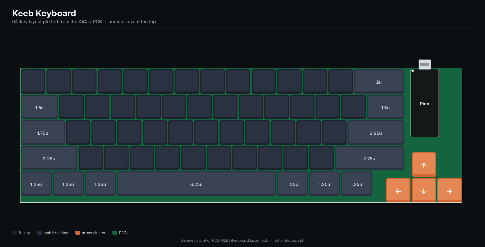
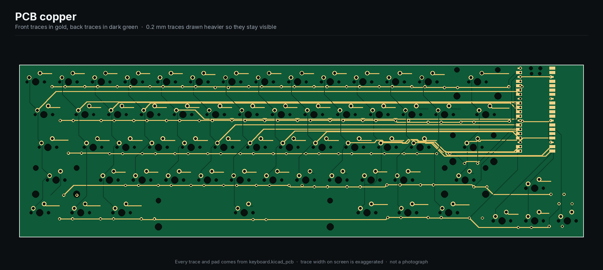
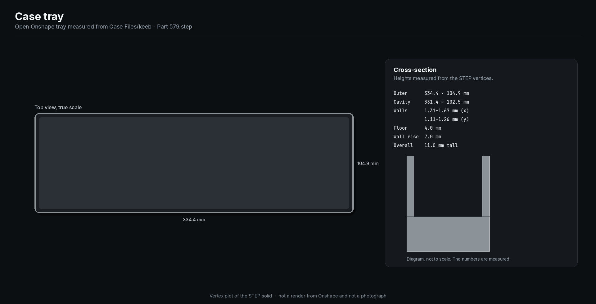
In KiCad's default Y-up view the number row sits toward the bottom of the canvas. The plots above put that row at the top, which is how the board sits on a desk. USB leaves the far edge.
PCB FILES/Output.zip, exported from KiCad 10.0.4.Unit sizes below are read from the footprints. The schematic does not store key legends, so this README does not invent a QWERTY print. The sizes themselves match an ANSI 60%.
| Row | Keys | Widths, left to right |
|---|---|---|
| 0 | 14 | 13 × 1u, 2u |
| 1 | 14 | 1.5u, 12 × 1u, 1.5u |
| 2 | 13 | 1.75u, 11 × 1u, 2.25u |
| 3 | 12 | 2.25u, 10 × 1u, 2.75u |
| 4 | 7 | 1.25u × 3, 6.25u, 1.25u × 3 |
| Arrows | 4 | 1u up, then 1u left / down / right, set slightly below the right side |
The Pico occupies the empty bay to the right of rows 0–2, above the arrow cluster.
| Piece | Choice |
|---|---|
| Schematic and PCB | KiCad 10.0.4 |
| Switch footprints | Switch_Keyboard_Cherry_MX:SW_Cherry_MX_PCB_* |
| Stabilizers | marbastlib STAB_MX_2u and STAB_MX_6.25u |
| Diodes | Device:D_Small on Diode_THT:D_DO-35_SOD27_P7.62mm_Horizontal |
| Microcontroller | Raspberry Pi Pico, Module:RaspberryPi_Pico_Common_Unspecified |
| Case | Onshape, exported as STEP AP242 |
| Firmware | Not in this repo yet. KEEB's firmware guide points at RMK. Any scanner that can drive a COL2ROW matrix can use the pinout below. |
| CI | GitHub Actions runs scripts/check_design.py (Python stdlib only) |
https://raw.githubusercontent.com/ebastler/ebastler-KiCad-repository/main/repository.json, then install marbastlib. The KEEB doc Designing the PCB has the click path..kicad_pro in the repo.PCB FILES/keyboard.kicad_sch
PCB FILES/keyboard.kicad_pcbpython3 scripts/check_design.pydocs/images/:pip install pillow
python3 scripts/render_previews.pyNo environment variables are required. See .env.example.
Switches are SW1–SW64, diodes D1–D64, stabilizers ST14, ST41, ST42, ST53, and ST58, and the Pico is A1. Rows and columns are global labels (ROW0–ROW4, COL0–COL16).
PCB FILES/Output.zip is a KiCad 10.0.4 fabrication set:
| File | Layer |
|---|---|
keyboard-F_Cu.gbr / keyboard-B_Cu.gbr | Front and back copper |
keyboard-F_Mask.gbr / keyboard-B_Mask.gbr | Solder mask |
keyboard-F_Silkscreen.gbr / keyboard-B_Silkscreen.gbr | Silkscreen |
keyboard-F_Paste.gbr / keyboard-B_Paste.gbr | Paste (empty of parts; this is a through-hole board) |
keyboard-Edge_Cuts.gbr | Board outline, 328.5 × 100.5 mm |
keyboard-PTH.drl / keyboard-NPTH.drl | Plated and non-plated drills |
Ask the fab for a 2-layer, 1.6 mm board. Traces are 0.2 mm and the two vias are a 0.3 mm drill in a 0.6 mm pad, so check the fab's minimums before you order. Details are in SECURITY.md.
| Qty | Refs | Part | Footprint |
|---|---|---|---|
| 64 | SW1–SW64 | MX-compatible PCB-mount switch | Cherry MX PCB, see the layout table for sizes |
| 64 | D1–D64 | Small-signal diode, DO-35 (KEEB uses 1N4148) | Horizontal, 7.62 mm pitch |
| 4 | ST14, ST41, ST42, ST53 | PCB-mount MX stabilizer, 2u | marbastlib STAB_MX_2u |
| 1 | ST58 | PCB-mount MX stabilizer, 6.25u | marbastlib STAB_MX_6.25u |
| 1 | A1 | Raspberry Pi Pico (Pico W and Pico 2 fit the same footprint) | Common Pico module |
| 1 | — | Keycaps to match the unit sizes | — |
| 1 | — | Case tray, or print/cut your own from the STEP | Onshape part |
The schematic symbol for the diode is D_Small, not a locked manufacturer part number. Match the DO-35 footprint.
Diode footprint pin 1 is the cathode and lands on the row. The switch connects the column to the diode anode. Drive columns, read rows (COL2ROW).
GPIO names are the official Raspberry Pi Pico pinout for these pad numbers. The unused pads in the KiCad footprint use that same numbering (GPIO22-Pad29, GPIO26_ADC0-Pad31, and so on).
| Net | Pico pin | GPIO |
|---|---|---|
| ROW0 | 1 | GP0 |
| ROW1 | 2 | GP1 |
| ROW2 | 4 | GP2 |
| ROW3 | 5 | GP3 |
| ROW4 | 6 | GP4 |
| COL0 | 7 | GP5 |
| COL1 | 9 | GP6 |
| COL2 | 10 | GP7 |
| COL3 | 11 | GP8 |
| COL4 | 12 | GP9 |
| COL5 | 14 | GP10 |
| COL6 | 15 | GP11 |
| COL7 | 16 | GP12 |
| COL8 | 17 | GP13 |
| COL9 | 19 | GP14 |
| COL10 | 20 | GP15 |
| COL11 | 21 | GP16 |
| COL12 | 22 | GP17 |
| COL13 | 24 | GP18 |
| COL14 | 25 | GP19 |
| COL15 | 26 | GP20 |
| COL16 | 27 | GP21 |
Pico pins 3, 8, 13, 18, 23, 28, and 38 are ground and are tied together on the module footprint. GP22, the ADC pins, RUN, 3V3, and VBUS stay on the module. That is what you want when the Pico's own regulator and USB connector do the power.
Import Case Files/keeb - Part 579.step into Onshape, Fusion 360, or FreeCAD. The solid is one open tray: 334.4 × 104.9 × 11.0 mm outside, with a cavity 331.4 × 102.5 mm, a 4 mm floor, and walls that rise 7 mm. Wall thickness is uneven, about 1.3–1.7 mm along the length and 1.1–1.3 mm along the depth. The PCB (328.5 × 100.5 mm) drops into that cavity. The original plan is glue plus PE foam, which matches a board with no mounting holes.
.
├── PCB FILES/
│   ├── keyboard.kicad_sch    # schematic, KiCad 10
│   ├── keyboard.kicad_pcb     # 2-layer board
│   └── Output.zip             # Gerbers and drills
├── Case Files/
│   └── keeb - Part 579.step   # Onshape tray
├── docs/images/               # plots generated from those files
├── scripts/
│   ├── check_design.py        # CI check, stdlib only
│   └── render_previews.py     # rebuild the plots (needs Pillow)
├── .github/                   # CI, issue forms, pull request template
├── LICENSE                    # MIT
├── CONTRIBUTING.md
├── CODE_OF_CONDUCT.md
├── SECURITY.md
└── .env.example               # no secrets; nothing reads this
Folder names keep the spaces they were published with.
Keeb Keyboard is an open-source 64-key mechanical keyboard design by Ryan Editraj. It is a KiCad PCB for a Raspberry Pi Pico, plus an Onshape case, published for Hack Club KEEB.
The alpha block is a 60-key ANSI 60% (right shift is 2.75u, so there is no extra 1u key beside it). Four arrow keys bring the switch count to 64. It is not a 65% or a 75%.
A Raspberry Pi Pico, soldered on the front of the board in the top-right bay. The footprint also fits a Pico W or a Pico 2. The matrix uses GP0 through GP21. Wireless pins are unused.
MX-compatible PCB-mount switches in Cherry MX footprints, one DO-35 small-signal diode per switch, and PCB-mount MX stabilizers on the wide keys. The KEEB build guide uses 1N4148 diodes for this footprint.
Install KiCad 10 or newer and marbastlib, then open PCB FILES/keyboard.kicad_sch and PCB FILES/keyboard.kicad_pcb. There is no KiCad project file to double-click.
You can't yet. Firmware is not in the repository. The matrix pinout is the map a firmware needs. Hack Club's guide recommends RMK.
Yes. The Gerbers and drills are in PCB FILES/Output.zip. It is a 2-layer, 1.6 mm, through-hole keyboard PCB, 328.5 × 100.5 mm. Read the fabrication notes before ordering: thin traces, small vias, no mounting holes.
Case Files/keeb - Part 579.step is a single Onshape tray, roughly 334 × 105 × 11 mm, sized to hold the PCB with glue and PE foam. It is not a full sandwich case and it has no switch plate.
No. The design files, Gerbers, STEP file, and git history were scanned. Nothing needs to be rotated. Manufacturing files are public on purpose.
Anyone. The design is MIT licensed. Keep the copyright notice if you redistribute it.
Ryan Editraj, while learning schematic capture, PCB layout, and CAD for Hack Club KEEB. The Pico is on the front of the board because mounting it on the back was not obvious yet, and the journaling habit started late in the build.
See CONTRIBUTING.md. Small, specific pull requests are the useful ones: a footprint fix, a regenerated Gerber zip, firmware that matches this matrix, or a clearer note. Please follow the Code of Conduct.
MIT © 2026 Ryan Editraj.
Ryan Editraj — AI builder and tech creator.
| Qty | Value | Footprint | References |
|---|---|---|---|
| 64 | D | Diode_THT:D_DO-35_SOD27_P7.62mm_Horizontal | D1, D2, D10, D11, D12, D13, D14, D15, D16, D17, D18, D19, D20, D21, D22, D23 +48 |
| 50 | SW_Push | Switch_Keyboard_Cherry_MX:SW_Cherry_MX_PCB_1.00u | SW1, SW2, SW10, SW11, SW12, SW13, SW16, SW17, SW18, SW19, SW20, SW21, SW22, SW23, SW24, SW25 +34 |
| 6 | SW_Push | Switch_Keyboard_Cherry_MX:SW_Cherry_MX_PCB_1.25u | SW55, SW56, SW57, SW59, SW60, SW61 |
| 4 | SW_stab | PCM_marbastlib-mx:STAB_MX_2u | ST14, ST41, ST42, ST53 |
| 2 | SW_Push | Switch_Keyboard_Cherry_MX:SW_Cherry_MX_PCB_1.50u | SW15, SW28 |
| 2 | SW_Push | Switch_Keyboard_Cherry_MX:SW_Cherry_MX_PCB_2.25u | SW41, SW42 |
| 1 | RaspberryPi_Pico | Module:RaspberryPi_Pico_Common_Unspecified | A1 |
| 1 | SW_Push | Switch_Keyboard_Cherry_MX:SW_Cherry_MX_PCB_2.75u | SW53 |
| 1 | SW_Push | Switch_Keyboard_Cherry_MX:SW_Cherry_MX_PCB_2.00u | SW14 |
| 1 | SW_Push | Switch_Keyboard_Cherry_MX:SW_Cherry_MX_PCB_6.25u | SW58 |
| 1 | SW_Push | Switch_Keyboard_Cherry_MX:SW_Cherry_MX_PCB_1.75u | SW29 |
| 1 | SW_stab | PCM_marbastlib-mx:STAB_MX_6.25u | ST58 |
It measures 328.5 × 100.5 mm and has 2 copper layers, 1.6 mm thick.
134 parts. The full list of its parts is on this page, with links to each part's symbol and footprint where PCBKit's library has them.
From the ryaneditraj/Keeb-Keyboard repository on GitHub, at the commit this page was made from: the board is PCB FILES/keyboard.kicad_pcb and its schematic PCB FILES/keyboard.kicad_sch. PCBKit opens the board in the browser, with nothing to install.
Its repository publishes it under the MIT licence: you may reuse it on that licence's terms (keep the author's notice, and for a copyleft licence share your changes alike).


ThomasVDD/SmartSupply
SmartSupply is a digital battery powered lab powersupply. It is Arduino compatible and can be controlled via PC over USB.


richardeoin/ax
This repository contains hardware and software for the AX5043 and AX5243 radios from AxSemi (now ON Semiconductor). They are probably the same die, but the AX5243 has fewer pins.