4 layers184.2 × 169.5 mm

 rweather/generic-front-panel2
Generic Front Panel for Hombrew Computers
Generic front panel is an open-source printed circuit board by rweather, from the rweather/generic-front-panel repository on GitHub, published under the MIT licence. It is a 2-layer board of 194.9 × 90.2 mm with 74 parts on 162 nets, routed with 1,679 tracks and 56 vias.
It is built around the 74HC244D, 74HC259D and 74HC138. Its parts include 20 switches, 14 ICs, 12 capacitors, 6 resistors and 6 diodes.


This repository contains schematics and other information for a generic front panel for 8-bit homebrew computers.
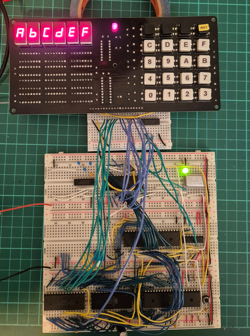
Here it is connected to my version of Ben Eater's 6502 Breadboard Computer, running the "hello.s" example from the "src/6502" directory. It is shown here after I typed ABCDEF on the keypad:
Here is a close-up of the front panel with a 3D-printed plate over the top:
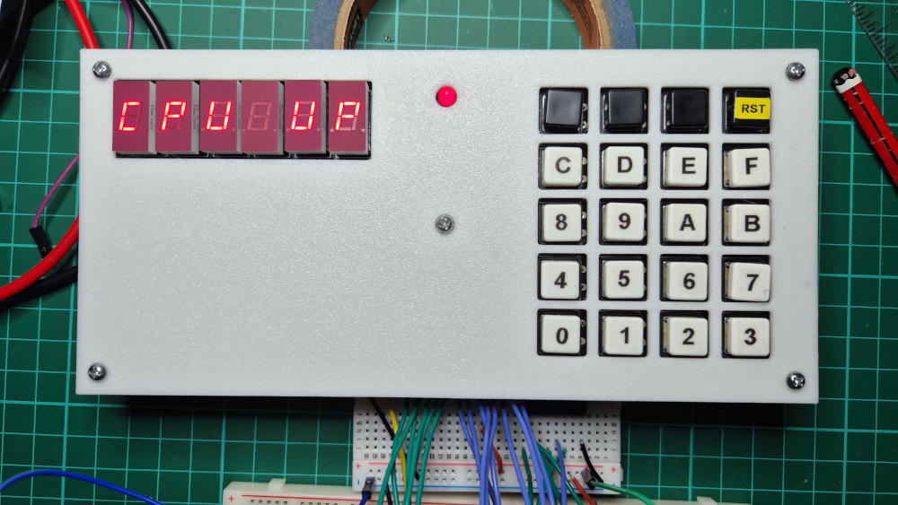
The "print" directory contains an OpenSCAD file for the 3D-printable plate. My brother, who is into 3D-printing, has a textured print bed for his printer. He printed the plate upside down and the texturing gave the plate a nice finish.
The generic front panel has the following features:
Note that this front panel requires software support. It doesn't directly operate the address bus, data bus, clock, and other control lines like front panels of old.
What this front panel does do is make it easy to write a memory monitor in software that can examine memory, modify memory, single-step, and so on. The 6 displays can display a 16-bit address and an 8-bit byte. Or anything else you like, even words.
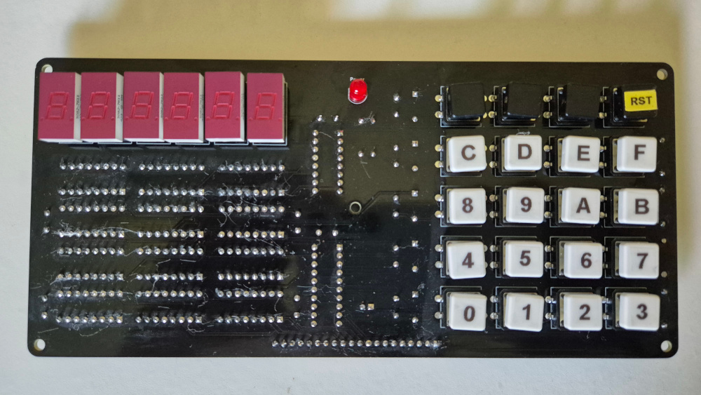
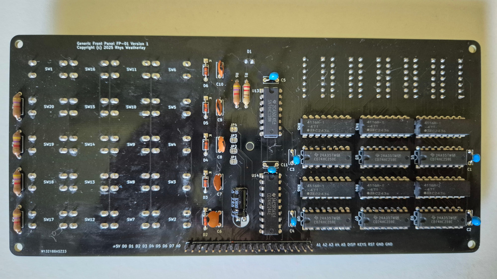
The seven segment displays, keypad buttons, and power LED are mounted on the front side of the PCB. All other components are mounted on the back side. The inline current limiting resistors are specified as 8-way resistor arrays. However, you could fit 8 regular resistors side by side instead.
The front panel draws about 250mA from the 5V rail when all 48 segments in the 7-segment displays and the power LED are lit. About 5mA per segment.
I have provided drivers and examples for various CPU's under the "src" directory. Patches welcome for other CPU's and homebrew boards.
The dimensions of the PCB are 195mm x 90mm. Five 3mm mounting holes are provided for mounting behind a face plate: four corners and one in the centre for added strength.
I recommend using DIP-14 sockets for the 7-segment LED displays to raise the height of the displays up to roughly level with the top of the push buttons plus keycaps. Sockets for the other IC's are up to you; I didn't bother.
Labels can be applied to the keycaps using a label maker and clear labels.
This is what the front and back of the PCB looks like once assembled (I had only done a very basic board clean at this point so it is still a little smudgy):
The connector on the bottom of the PCB has the following pins:
| Pin | Description |
| 1 | +5V |
| 2 | D0 |
| 3 | D1 |
| 4 | D2 |
| 5 | D3 |
| 6 | D4 |
| 7 | D5 |
| 8 | D6 |
| 9 | D7 |
| 10 | A0 |
| 11 | A1 |
| 12 | A2 |
| 13 | A3 |
| 14 | A4 |
| 15 | A5 |
| 16 | Select Display (active low) |
| 17 | Select Keypad (active low) |
| 18 | Reset (active low) |
| 19 | GND |
| 20 | GND |
To interface to your homebrew computer, you will need to provide address decoding for the two "chip select" lines "Select Display" and "Select Keypad".
You can put the front panel anywhere in memory or I/O space that is aligned on a 64-byte boundary. Only the bottom 6 address bits are provided to the front panel. You need to decode the upper 10 bits (of a 16-bit address) yourself by some means.
"Select Display" should be low when the top-most bits of the address match the location in memory where you want to put the display, and when the bus is in a write cycle. The display occupies 64 bytes of memory space.
"Select Keypad" should be low when the top-most bits of the address match the location in memory where you want to put the keypad, and when the bus is in a read cycle. The keypad occupies 32 bytes of memory space. It can overlap with the display in memory if that is easier.
Each segment of the display has its own memory address. Each digit occupies 8 bytes of memory space, for the segments A, B, C, D, E, F, G, and decimal point. The displays are at offsets 0, 8, 16, 24, 32, and 40 in the memory space.
Write a byte with the low bit set to 0 to a segment's address to turn the segment on, or write a byte with the low bit set to 1 to turn the segment off. The segment will stay lit until modified or the power is turned off. The display is not multiplexed so there is no need to constantly refresh.
Writing any byte value to offset 56 will turn all segments on. This can be useful for testing. Normally you will want to turn everything off at startup time.
The "one byte per segment" design was borrowed from the Heathkit ET-3400. 74HC259 addressable latches are used to individually address each segment, and to remember the state of the segment between writes.
The keypad consists of 5 rows of 4 keys. The rows are associated with address bits A0 to A4. Scan through the keypad one row at a time, setting one address bit to 0 and the rest to 1. When you read from that address, the bits that are set to zero indicate which keys are pressed on that row.
| Address | Bit | Key |
| $XX1E (A0) | 0 | 0 |
| $XX1E (A0) | 1 | 1 |
| $XX1E (A0) | 2 | 2 |
| $XX1E (A0) | 3 | 3 |
| $XX1D (A1) | 0 | 4 |
| $XX1D (A1) | 1 | 5 |
| $XX1D (A1) | 2 | 6 |
| $XX1D (A1) | 3 | 7 |
| $XX1B (A2) | 0 | 8 |
| $XX1B (A2) | 1 | 9 |
| $XX1B (A2) | 2 | A |
| $XX1B (A2) | 3 | B |
| $XX17 (A3) | 0 | C |
| $XX17 (A3) | 1 | D |
| $XX17 (A3) | 2 | E |
| $XX17 (A3) | 3 | F |
| $XX0F (A4) | 0 | CMD1 |
| $XX0F (A4) | 1 | CMD2 |
| $XX0F (A4) | 2 | CMD3 |
| $XX0F (A4) | 3 | (not used) |
The "Reset" key is special. It will pull pin 18 on the connector down to GND when pressed. It is assumed that a pull-up resistor and debouncing capacitor are present on your main computer board. If you want to use "Reset" for something else (such as a "CMD4" key), you can connect pin 18 to an I/O pin on your main computer board.
The "rows as addresses" design was borrowed from the VZ200 / Laser 200. Only a single 74HC244 bus transceiver is required to read the keypad. Everything else is pushbuttons, diodes, resistors, and capacitors.
There are jumpers on the back of the board that can be cut to wire up additional keys if you need more than 20. The extra keys will be available as bits 4 through 7. The bits are pulled high if the jumpers are uncut.
MIT License.
For more information on this project, to report bugs, or to suggest improvements, please contact the author Rhys Weatherley via email.
| Qty | Value | Footprint | References |
|---|---|---|---|
| 6 | 100nF | Capacitor_THT:C_Disc_D6.0mm_W2.5mm_P5.00mm | C1, C2, C3, C4, C5, C11 |
| 6 | 470R | Package_DIP:DIP-16_W7.62mm | RN1, RN2, RN3, RN4, RN5, RN6 |
| 6 | 74HC259 | Package_DIP:DIP-16_W7.62mm | U1, U2, U3, U7, U8, U9 |
| 6 | MAN71A | Display_7Segment:MAN71A | U4, U5, U6, U10, U11, U12 |
| 5 | 100pF | Capacitor_THT:C_Disc_D6.0mm_W2.5mm_P5.00mm | C6, C7, C8, C9, C10 |
| 5 | 1N4148 | Diode_THT:D_DO-35_SOD27_P7.62mm_Horizontal | D2, D3, D4, D5, D6 |
| 5 | 3mm | MountingHole:MountingHole_3mm | H1, H2, H3, H4, H5 |
| 5 | 4K7 | Resistor_THT:R_Axial_DIN0207_L6.3mm_D2.5mm_P10.16mm_Horizontal | R2, R3, R4, R5, R6 |
| 4 | ~ | Jumper:SolderJumper-2_P1.3mm_Bridged_RoundedPad1.0x1.5mm | JP1, JP2, JP3, JP4 |
| 1 | 0 | Button_Switch_THT:SW_PUSH-12mm | SW2 |
| 1 | 1 | Button_Switch_THT:SW_PUSH-12mm | SW7 |
| 1 | 100uF | Capacitor_THT:CP_Radial_D6.3mm_P2.50mm | C12 |
| 1 | 2 | Button_Switch_THT:SW_PUSH-12mm | SW12 |
| 1 | 220R | Resistor_THT:R_Axial_DIN0207_L6.3mm_D2.5mm_P10.16mm_Horizontal | R1 |
| 1 | 3 | Button_Switch_THT:SW_PUSH-12mm | SW17 |
| 1 | 4 | Button_Switch_THT:SW_PUSH-12mm | SW3 |
| 1 | 5 | Button_Switch_THT:SW_PUSH-12mm | SW8 |
| 1 | 6 | Button_Switch_THT:SW_PUSH-12mm | SW13 |
| 1 | 7 | Button_Switch_THT:SW_PUSH-12mm | SW18 |
| 1 | 74HC138 | Package_DIP:DIP-16_W7.62mm | U13 |
| 1 | 74HC244 | Package_DIP:DIP-20_W7.62mm | U14 |
| 1 | 8 | Button_Switch_THT:SW_PUSH-12mm | SW4 |
| 1 | 9 | Button_Switch_THT:SW_PUSH-12mm | SW9 |
| 1 | A | Button_Switch_THT:SW_PUSH-12mm | SW14 |
| 1 | B | Button_Switch_THT:SW_PUSH-12mm | SW19 |
| 1 | C | Button_Switch_THT:SW_PUSH-12mm | SW5 |
| 1 | CMD1 | Button_Switch_THT:SW_PUSH-12mm | SW6 |
| 1 | CMD2 | Button_Switch_THT:SW_PUSH-12mm | SW11 |
| 1 | CMD3 | Button_Switch_THT:SW_PUSH-12mm | SW16 |
| 1 | D | Button_Switch_THT:SW_PUSH-12mm | SW10 |
| 1 | E | Button_Switch_THT:SW_PUSH-12mm | SW15 |
| 1 | F | Button_Switch_THT:SW_PUSH-12mm | SW20 |
| 1 | Interface | Connector_PinSocket_2.54mm:PinSocket_1x20_P2.54mm_Vertical | J1 |
| 1 | Power | LED_THT:LED_D5.0mm | D1 |
| 1 | Reset | Button_Switch_THT:SW_PUSH-12mm | SW1 |
It measures 194.9 × 90.2 mm and has 2 copper layers, 1.6 mm thick.
74 parts, built around the 74HC244D, 74HC259D and 74HC138. The full list of its parts is on this page, with links to each part's symbol and footprint where PCBKit's library has them.
From the rweather/generic-front-panel repository on GitHub, at the commit this page was made from: the board is schematics/Generic_Front_Panel/Generic_Front_Panel.kicad_pcb and its schematic schematics/Generic_Front_Panel/Generic_Front_Panel.kicad_sch. PCBKit opens the board in the browser, with nothing to install.
Its repository publishes it under the MIT licence: you may reuse it on that licence's terms (keep the author's notice, and for a copyleft licence share your changes alike).


abzman/SMS-3D-glasses-genesis-cart-stack
pass-through adapter to add 3d glasses support to a genesis running master system software


Greentalinjo/74HController
A game controller built entirely from discrete 74HC logic - no microcontroller, a diode ROM and an 8-N-1 serial frame out of an RJ45 console port.

